Data transfer channel connecting parts of a computer
This article is about buses in computer hardware. For buses in software, see Software bus.
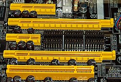
Four PCI Express bus card slots (from top to second from bottom: ×4, ×16, ×1 and ×16), compared to a 32-bit conventional PCI bus card slot (very bottom)
In computer architecture, a bus (historically also called a data highway[1] or databus) is a communication system that transfers data between components inside a computer or between computers.[2] It encompasses both hardware (e.g., wires, optical fiber) and software, including communication protocols.[3] At its core, a bus is a shared physical pathway, typically composed of wires, traces on a circuit board, or busbars, that allows multiple devices to communicate. To prevent conflicts and ensure orderly data exchange, buses rely on a communication protocol to manage which device can transmit data at a given time.
Buses are categorized based on their role, such as system buses (also known as internal buses, internal data buses, or memory buses) connecting the CPU and memory. Expansion buses, also called peripheral buses, extend the system to connect additional devices, including peripherals. Examples of widely used buses include PCI Express (PCIe) for high-speed internal connections and Universal Serial Bus (USB) for connecting external devices.
Modern buses utilize both parallel and serial communication, employing advanced encoding methods to maximize speed and efficiency. Features such as direct memory access (DMA) further enhance performance by allowing data transfers directly between devices and memory without requiring CPU intervention.
An address bus is a bus that is used to specify a physical address. When a processor or DMA-enabled device needs to read or write to a memory location, it specifies that memory location on the address bus (the value to be read or written is sent on the data bus).[4] The width of the address bus determines the amount of memory a system can transfer simultaneously.[5] For example, a system with a 32-bit address bus can address 232 (4,294,967,296) memory locations.[6] If each memory location holds one byte, the addressable memory space is about 4GB.
Address multiplexing
Early processors used a wire for each bit of the address width. For example, a 16-bit address bus had 16 physical wires making up the bus. As the buses became wider and longer, this approach became expensive in terms of the number of chip pins and board traces. Beginning with the Mostek 4096 DRAM, address multiplexing implemented with multiplexers became common.[7] In a multiplexed address scheme, the address is sent in two equal parts on alternate bus cycles. This halves the number of address bus signals required to connect to the memory. For example, a 32-bit address bus can be implemented by using 16 lines and sending the first half of the memory address, immediately followed by the second half memory address.
Typically two additional pins in the control bus–row-address strobe (RAS) and column-address strobe (CAS)–are used to tell the DRAM whether the address bus is currently sending the first half of the memory address or the second half.
Implementation
Accessing an individual byte frequently requires reading or writing the full bus width (a word) at once. In these instances, the least significant bits of the address bus may not even be implemented - it is instead the responsibility of the controlling device to isolate the individual byte required from the complete word transmitted. This is the case, for instance, with the VESA Local Bus, which lacks the two least significant bits, limiting this bus to aligned 32-bit transfers.
Historically, there were also some examples of computers that were only able to address words–word machines.
The memory bus is the bus that connects the main memory to the memory controller in computer systems. Originally, general-purpose buses like VMEbus and the S-100 bus were used, but to reduce latency, modern memory buses are designed to connect directly to DRAM chips, and thus are defined by chip standards bodies such as JEDEC. Examples are the various generations of SDRAM, and serial point-to-point buses like SLDRAM and RDRAM.
Implementation details
Buses can be parallel buses, which carry data words in parallel on multiple wires, or serial buses, which carry data in bit-serial form. The addition of extra power and control connections, differential drivers, and data connections in each direction usually means that most serial buses have more conductors than the minimum of one used in 1-Wire and UNI/O. As data rates increase, the problems of timing skew, power consumption, electromagnetic interference and crosstalk across parallel buses become more and more difficult to circumvent. One partial solution to this problem has been to double pump the bus. Often, a serial bus can be operated at higher overall data rates than a parallel bus, despite having fewer electrical connections, because a serial bus inherently has no timing skew or crosstalk. USB, FireWire, and Serial ATA are examples of this. Multidrop connections do not work well for fast serial buses, so most modern serial buses use daisy-chain or hub designs.
The transition from parallel to serial buses was allowed by Moore's law which allowed for the incorporation of serializer/deserializers in integrated circuits which are used in computers.[8]
Network connections such as Ethernet are not generally regarded as buses, although the difference is largely conceptual rather than practical. An attribute generally used to characterize a bus is that power is provided by the bus for the connected hardware. This emphasizes the busbar origins of bus architecture as supplying switched or distributed power. This excludes, as buses, schemes such as serial RS-232, parallel Centronics, IEEE 1284 interfaces and Ethernet, since these devices also needed separate power supplies. Universal Serial Bus devices may use the bus-supplied power, but often use a separate power source. This distinction is exemplified by a telephone system with a connected modem, where the RJ11 connection and associated modulated signalling scheme is not considered a bus, and is analogous to an Ethernet connection. A phone line connection scheme is not considered to be a bus with respect to signals, but the Central Office uses buses with cross-bar switches for connections between phones.
However, this distinction—that power is provided by the bus—is not the case in many avionic systems, where data connections such as ARINC 429, ARINC 629, MIL-STD-1553B (STANAG 3838), and EFABus (STANAG 3910) are commonly referred to as data buses or, sometimes, databuses. Such avionic data buses are usually characterized by having several Line Replaceable Items/Units (LRI/LRUs) connected to a common, shared media. They may, as with ARINC 429, be simplex, i.e. have a single source LRI/LRU or, as with ARINC 629, MIL-STD-1553B, and STANAG 3910, be duplex, allowing all the connected LRI/LRUs to act, at different times (half duplex), as transmitters and receivers of data.[9]
The frequency or the speed of a bus is measured in Hz, such as MHz, and determines how many clock cycles there are per second; there can be one or more data transfers per clock cycle. If there is a single transfer per clock cycle, it is known as Single Data Rate (SDR), and if there are two transfers per clock cycle, it is known as Double Data Rate (DDR) although the use of signaling other than SDR is uncommon outside of RAM. An example of this is PCIe, which uses SDR.[10] Within each data transfer, there can be multiple bits of data. This is described as the width of a bus, which is the number of bits the bus can transfer per clock cycle and can be synonymous with the number of physical electrical conductors the bus has if each conductor transfers one bit at a time.[11][12][13] The data rate in bits per second can be obtained by multiplying the number of bits per clock cycle times the frequency times the number of transfers per clock cycle.[14][15] Alternatively a bus such as PCIe can use modulation or encoding such as PAM4[16][17][18] which groups 2 bits into symbols which are then transferred instead of the bits themselves, and allows for an increase in data transfer speed without increasing the frequency of the bus. The effective or real data transfer speed/rate may be lower due to the use of encoding that also allows for error correction, such as 128/130b (b for bit) encoding.[19][20][10] The data transfer speed is also known as the bandwidth.[21][22]
The simplest system bus has completely separate input data lines, output data lines, and address lines. To reduce cost, most microcomputers have a bidirectional data bus, re-using the same wires for input and output at different times.[23]
Some processors use a dedicated wire for each bit of the address bus, data bus, and control bus. For example, the 64-pin STEbus is composed of 8 physical wires dedicated to the 8-bit data bus, 20 physical wires dedicated to the 20-bit address bus, 21 physical wires dedicated to the control bus, and 15 physical wires dedicated to various power buses.
Bus multiplexing requires fewer wires, which reduces costs in many early microprocessors and DRAM chips. One common multiplexing scheme, address multiplexing, has already been mentioned. Another multiplexing scheme re-uses the address bus pins as the data bus pins,[23] an approach used by conventional PCI and the 8086. The various serial buses can be seen as the ultimate limit of multiplexing, sending each of the address bits and each of the data bits, one at a time, through a single pin (or a single differential pair).
History
Over time, several groups of people worked on various computer bus standards, including the IEEE Bus Architecture Standards Committee (BASC), the IEEE Superbus study group, the open microprocessor initiative (OMI), the open microsystems initiative (OMI), the Gang of Nine that developed EISA, etc.[citation needed]
First generation
Early computer buses were bundles of wire that attached computer memory and peripherals. Anecdotally termed the digit trunk in the early Australian CSIRAC computer,[24] they were named after electrical power buses, or busbars. Almost always, there was one bus for memory, and one or more separate buses for peripherals. These were accessed by separate instructions, with completely different timings and protocols.
One of the first complications was the use of interrupts. Early computer programs performed I/O by waiting in a loop for the peripheral to become ready. This was a waste of time for programs that had other tasks to do. Also, if the program attempted to perform those other tasks, it might take too long for the program to check again, resulting in loss of data. Engineers thus arranged for the peripherals to interrupt the CPU. The interrupts had to be prioritized because the CPU can only execute code for one peripheral at a time, and some devices are more time-critical than others.
High-end systems introduced the idea of channel controllers, which were essentially small computers dedicated to handling the input and output of a given bus. IBM introduced these on the IBM 709 in 1958, and they became a common feature of their platforms. Other high-performance vendors like Control Data Corporation implemented similar designs. Generally, the channel controllers would do their best to run all of the bus operations internally, moving data when the CPU was known to be busy elsewhere if possible, and only using interrupts when necessary. This greatly reduced CPU load and provided better overall system performance.
To provide modularity, memory and I/O buses can be combined into a unified system bus.[25] In this case, a single mechanical and electrical system can be used to connect together many of the system components, or in some cases, all of them.
Later computer programs began to share memory common to several CPUs. Access to this memory bus had to be prioritized, as well. The simple way to prioritize interrupts or bus access was with a daisy chain. In this case, signals will naturally flow through the bus in physical or logical order, eliminating the need for complex scheduling.
Early microcomputer bus systems were essentially a passive backplane connected directly or through buffer amplifiers to the pins of the CPU. Memory and other devices would be added to the bus using the same address and data pins as the CPU itself used, connected in parallel. Communication was controlled by the CPU, which read and wrote data from the devices as if they are blocks of memory, using the same instructions, all timed by a central clock controlling the speed of the CPU. Still, devices interrupted the CPU by signaling on separate CPU pins.
For instance, a disk drive controller would signal the CPU that new data was ready to be read, at which point the CPU would move the data by reading the memory location that corresponded to the disk drive. Almost all early microcomputers were built in this fashion, starting with the S-100 bus in the Altair 8800 computer system.
In some instances, most notably in the IBM PC, although similar physical architecture can be employed, instructions to access peripherals (in and out) and memory (mov and others) have not been made uniform at all, and still generate distinct CPU signals, that could be used to implement a separate I/O bus.
These simple bus systems had a serious drawback when used for general-purpose computers. All the equipment on the bus had to talk at the same speed, as it shared a single clock.
Increasing the speed of the CPU becomes harder because the speed of all the devices must increase as well. When it is not practical or economical to have all devices as fast as the CPU, the CPU must either enter a wait state, or work at a slower clock frequency temporarily,[27] to talk to other devices in the computer. While acceptable in embedded systems, this problem was not tolerated for long in general-purpose, user-expandable computers.
Such bus systems are also difficult to configure when constructed from common off-the-shelf equipment. Typically, each added expansion card requires many jumpers in order to set memory addresses, I/O addresses, interrupt priorities, and interrupt numbers.
Second-generation bus systems like NuBus addressed some of these problems. They typically separated the computer into two address spaces, the CPU and memory on one side, and the various peripheral devices on the other. A bus controller accepted data from the CPU side to be moved to the peripherals side, thus shifting the communications protocol burden from the CPU itself. This allowed the CPU and memory side to evolve separately from the peripheral bus. Devices on the bus could talk to each other with no CPU intervention. This led to much better performance but also required the cards to be much more complex. These buses also often addressed speed issues by being bigger in terms of the size of the data path, moving from 8-bit parallel buses in the first generation, to 16 or 32-bit in the second, as well as adding software setup (later standardized as Plug-n-play) to supplant or replace the jumpers.
However, these newer systems shared one quality with their earlier cousins, in that everyone on the bus had to talk at the same speed. While the CPU was now isolated and could increase speed, CPUs and memory continued to increase in speed much faster than the buses they talked to. The result was that the bus speeds were now much slower than what a modern system needed, and the machines were left starved for data. A particularly common example of this problem was that video cards quickly outran even the newer bus systems like PCI, and computers began to include AGP just to drive the video card. By 2004, AGP was outgrown again by high-end video cards and other peripherals and had been replaced by the new PCI Express bus.
An increasing number of external devices started employing their own bus systems as well. When disk drives were first introduced, they would be added to the machine with a card plugged into the bus, which is why computers have so many slots on the bus. But through the 1980s and 1990s, new systems like SCSI and IDE were introduced to serve this need, leaving most slots in modern systems empty. Today, there are likely to be about five different buses in the typical machine, supporting various devices.[citation needed]
Third-generation buses have been emerging into the market since about 2001, including HyperTransport and InfiniBand. They also tend to be very flexible in terms of their physical connections, allowing them to be used both as internal buses as well as connecting different machines together. This can lead to complex problems when trying to service different requests, so much of the work on these systems concerns software design, as opposed to the hardware itself. In general, these third-generation buses tend to look more like a network than the original concept of a bus, with a higher protocol overhead needed than early systems, while also allowing multiple devices to use the bus at once.
Buses such as Wishbone have been developed by the open source hardware movement in an attempt to further remove legal and patent constraints from computer design.
IEEE-488 (also known as GPIB, General-Purpose Interface Bus, and HPIB, Hewlett-Packard Instrumentation Bus)
PC Card, previously known as PCMCIA, much used in laptop computers and other portables, but fading with the introduction of USB and built-in network and modem connections
Serial
Many field buses are serial data buses (not to be confused with the parallel data bus section of a system bus or expansion card), several of which use the RS-485 electrical characteristics and then specify their own protocol and connector:
↑Avionic Systems Standardisation Committee, Guide to Digital Interface Standards For Military Avionic Applications, ASSC/110/6/2, Issue 2, September 2003
↑C. Gordon Bell; R. Cady; H. McFarland; B. Delagi; J. O'Laughlin; R. Noonan; W. Wulf (1970). A New Architecture for Mini-Computers—The DEC PDP-11(PDF). Spring Joint Computer Conference. pp.657–675. Archived(PDF) from the original on 2011-11-27.
This page is based on this Wikipedia article Text is available under the CC BY-SA 4.0 license; additional terms may apply. Images, videos and audio are available under their respective licenses.