SPI follows a master–slave architecture,[1] where a device (variously called master, leader, controller, main...) orchestrates communication with one or more devices (variously called slave, follower, target, sub...) by driving the clock and chip select signals. As there is no formal standard, some manufacturer introduces devices with the ability to change their roles on the fly.
Motorola's original specification (from the early 1980s) uses four logic signals, aka lines or wires, to support full duplex communication. It is sometimes called a four-wireserial bus to contrast with three-wire variants which are half duplex, and with the two-wireI²C and 1-Wire serial buses.
MOSI on a master outputs to MOSI on a slave. MISO on a slave outputs to MISO on a master.
Each device internally uses a shift register for serial communication, which together forms an inter-chip circular buffer.
To support multidrop bus, slave devices should use tri-state outputs so their MISO signal becomes high impedance (electrically disconnected) when the device is not selected. Slaves without tri-state outputs cannot share a MISO line with other slaves without using an external tri-state buffer.
Data transmission
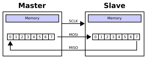
A typical hardware setup using two shift registers to form an inter-chip circular bufferSerial Peripheral Interface animation. This animation shows a scenario where the master sends 8-bit data and simultaneously reads 16-bit data from the slave. The lower boxes represent the device's memories.
To begin communication, the SPI master first selects the device he want to communicate with by pulling its SS low. (The bar above SS indicates it is an active low signal, so a low voltage means "selected", while a high voltage means "not selected")
If a waiting period is required, such as for an analog-to-digital conversion, the master must wait for at least that period of time before issuing clock cycles.[note 2]
During each SPI clock cycle, full-duplex transmission of a single bit occurs. The master sends a bit on the MOSI line while the slave sends a bit on the MISO line, and then each reads their corresponding incoming bit. This sequence is maintained even when only one-directional data transfer is intended.
Transmission using a single slave involves one shift register in the master and one shift register in the slave, both of some given word size (e.g. 8 bits). The transmissions often consist of eight-bit words, but other word-sizes are also common, for example, sixteen-bit words for touch-screen controllers or audio codecs, such as the TSC2101 by Texas Instruments, or twelve-bit words for many digital-to-analog or analog-to-digital converters.
Data is usually shifted out with the most-significant bit (MSB) first but the original specification has a LSBFE ("LSB-First Enable") to control whether data is transferred least (LSB) or most significant bit (MSB) first. On the clock edge, both master and slave shift out a bit to its counterpart. On the next clock edge, each receiver samples the transmitted bit and stores it in the shift register as the new least-significant bit. After all bits have been shifted out and in, the master and slave have exchanged register values. If more data needs to be exchanged, the shift registers are reloaded and the process repeats. Transmission may continue for any number of clock cycles. When complete, the master stops toggling the clock signal, and typically deselects the slave.
If a single slave device is used, its SS pin may be fixed to logic low if the slave permits it. With multiple slave devices, a multidrop configuration requires an independent SS signal from the master for each slave device, while a daisy-chain configuration only requires one SS signal.
Every slave on the bus that has not been selected should disregard the input clock and MOSI signals. And to prevent contention on MISO, non-selected slaves must use tristate output. Slaves that are not already tristate will need external tristate buffers to ensure this.[3]
Clock polarity and phase
In addition to setting the clock frequency, the master must also configure the clock polarity and phase with respect to the data. Motorola[4][5] named these two options as CPOL and CPHA (for clock polarity and clock phase) respectively, a convention most vendors have also adopted.
SPI timing diagram for both clock polarities and phases. Data bits output on blue lines if CPHA=0, or on red lines if CPHA=1, and sample on opposite-colored lines. Numbers identify data bits. Z indicates high impedance.
The SPI timing diagram shown is further described below:
CPOL represents the polarity of the clock. Polarities can be converted with a simple inverter.
SCLKCPOL=0 is a clock which idles at the logical low voltage.
SCLKCPOL=1 is a clock which idles at the logical high voltage.
CPHA represents the phase of each data bit's transmission cycle relative to SCLK.
For CPHA=0:
The first data bit is output immediately when SS activates.
Subsequent bits are output when SCLK transitions to its idle voltage level.
Sampling occurs when SCLK transitions from its idle voltage level.
For CPHA=1:
The first data bit is output on SCLK's first clock edge afterSS activates.
Subsequent bits are output when SCLK transitions from its idle voltage level.
Sampling occurs when SCLK transitions to its idle voltage level.
Conversion between these two phases is non-trivial.
MOSI and MISO signals are usually stable (at their reception points) for the half cycle until the next bit's transmission cycle starts, so SPI master and slave devices may sample data at different points in that half cycle, for flexibility, despite the original specification.
Mode numbers
The combinations of polarity and phases are referred to by these "SPI mode" numbers with CPOL as the high order bit and CPHA as the low order bit:
SPI mode
Clock polarity (CPOL)
Clock phase (CPHA)
Data is shifted out on
Data is sampled on
0
0
0
falling SCLK, and when SS activates
rising SCLK
1
0
1
rising SCLK
falling SCLK
2
1
0
rising SCLK, and when SS activates
falling SCLK
3
1
1
falling SCLK
rising SCLK
Notes:
Another commonly used notation represents the mode as a (CPOL, CPHA) tuple; e.g., the value '(0, 1)' would indicate CPOL=0 and CPHA=1.
In Full Duplex operation, the master device could transmit and receive with different modes. For instance, it could transmit in Mode 0 and be receiving in Mode 1 at the same time.
Different vendors may use different naming schemes, like CKE for clock edge or NCPHA for the inversion of CPHA.
Valid communications
Some slave devices are designed to ignore any SPI communications in which the number of clock pulses is greater than specified. Others do not care, ignoring extra inputs and continuing to shift the same output bit. It is common for different devices to use SPI communications with different lengths, as, for example, when SPI is used to access an IC's scan chain by issuing a command word of one size (perhaps 32 bits) and then getting a response of a different size (perhaps 153 bits, one for each pin in that scan chain).
Interrupts
Interrupts are outside the scope of SPI; their usage is neither forbidden nor specified, and so may be implemented optionally.
From master to slave
Microcontrollers configured as slave devices may have hardware support for generating interrupt signals to themselves when data words are received or overflow occurs in a receive FIFO buffer,[6] and may also set up an interrupt routine when their slave select input line is pulled low or high.
Though the previous operation section focused on a basic interface with a single slave, SPI can instead communicate with multiple slaves using multidrop, daisy chain, or expander configurations.
Multidrop configuration
Multidrop SPI bus
In the multidrop bus configuration, each slave has its own SS, and the master selects only one at a time. MISO, SCLK, and MOSI are each shared by all devices. This is the way SPI is normally used.
Since the MISO pins of the slaves are connected together, they are required to be tri-state pins (high, low or high-impedance), where the high-impedance output must be applied when the slave is not selected. Slave devices not supporting tri-state may be used in multidrop configuration by adding a tri-state buffer chip controlled by its SS signal.[3] (Since only a single signal line needs to be tristated per slave, one typical standard logic chip that contains four tristate buffers with independent gate inputs can be used to interface up to four slave devices to an SPI bus)
Caveat: All SS signals should start high (to indicate no slaves are selected) before sending initialization messages to any slave, so other uninitialized slaves ignore messages not addressed to them. This is a concern if the master uses general-purpose input/output (GPIO) pins (which may default to an undefined state) for SS and if the master uses separate software libraries to initialize each device. One solution is to configure all GPIOs used for SS to output a high voltage for all slaves before running initialization code from any of those software libraries. Another solution is to add a pull-up resistor on each SS, to ensure that all SS signals are initially high.[3]
Daisy chain configuration
Daisy-chained SPI
Some products that implement SPI may be connected in a daisy chain configuration, where the first slave's output is connected to the second slave's input, and so on with subsequent slaves, until the final slave, whose output is connected back to the master's input. This effectively merges the individual communication shift registers of each slave to form a single larger combined shift register that shifts data through the chain. This configuration only requires a single SS line from the master, rather than a separate SS line for each slave.[7]
In addition to using SPI-specific slaves, daisy-chained SPI can include discrete shift registers for more pins of inputs (e.g. using the parallel-in serial-out74 xx165)[8] or outputs (e.g. using the serial-in parallel-out74 xx595)[9] chained indefinitely. Other applications that can potentially interoperate with daisy-chained SPI include SGPIO, JTAG,[10] and I2C.
Expander configurations
Expander configurations use SPI-controlled addressing units (e.g. binary decoders, demultiplexers, or shift registers) to add chip selects.
For example, one SS can be used for transmitting to a SPI-controlled demultiplexer an index number controlling its select signals, while another SS is routed through that demultiplexer according to that index to select the desired slave.[11]
Pros and cons
Advantages
Full duplex communication in the default version of this protocol
Board real estate and wiring savings compared to a parallel bus are significant, and have earned SPI a solid role in embedded systems. That is true for most system-on-a-chip processors, both with higher-end 32-bit processors such as those using ARM, MIPS, or PowerPC and with lower-end microcontrollers such as the AVR, PIC, and MSP430. These chips usually include SPI controllers capable of running in either master or slave mode. In-system programmable AVR controllers (including blank ones) can be programmed using SPI.[12]
Chip or FPGA based designs sometimes use SPI to communicate between internal components; on-chip real estate can be as costly as its on-board cousin. And for high-performance systems, FPGAs sometimes use SPI to interface as a slave to a host, as a master to sensors, or for flash memory used to bootstrap if they are SRAM-based.
The full-duplex capability makes SPI very simple and efficient for single master/single slave applications. Some devices use the full-duplex mode to implement an efficient, swift data stream for applications such as digital audio, digital signal processing, or telecommunications channels, but most off-the-shelf chips stick to half-duplex request/response protocols.
Variations
SPI implementations have a wide variety of protocol variations. Some devices are transmit-only; others are receive-only. Slave selects are sometimes active-high rather than active-low. Some devices send the least-significant bit first. Signal levels depend entirely on the chips involved. And while the baseline SPI protocol has no command codes, every device may define its own protocol of command codes. Some variations are minor or informal, while others have an official defining document and may be considered to be separate but related protocols.
Original definition
Motorola in 1983 listed[13] three 6805 8-bit microcomputers that have an integrated "Serial Peripheral Interface", whose functionality is described in a 1984 manual.[14]
AN991
Motorola's 1987 Application Node AN991 "Using the Serial Peripheral Interface to Communicate Between Multiple Microcomputers"[15] (now under NXP, last revised 2002[5]) informally serves as the "official" defining document for SPI.
Timing variations
Some devices have timing variations from Motorola's CPOL/CPHA modes. Sending data from slave to master may use the opposite clock edge as master to slave. Devices often require extra clock idle time before the first clock or after the last one, or between a command and its response.
Some devices have two clocks, one to read data, and another to transmit it into the device. Many of the read clocks run from the slave select line.
Transmission size
Different transmission word sizes are common. Many SPI chips only support messages that are multiples of 8 bits. Such chips can not interoperate with the JTAG or SGPIO protocols, or any other protocol that requires messages that are not multiples of 8 bits.
No slave select
Some devices do not use slave select, and instead manage protocol state machine entry/exit using other methods.
Connectors
Anyone needing an external connector for SPI defines their own or uses another standard connection such as: UEXT, Pmod, various JTAG connectors, Secure Digital card socket, etc.
Flow control
Some devices require an additional flow control signal from slave to master, indicating when data is ready. This leads to a 5-wire protocol instead of the usual 4. Such a ready or enable signal is often active-low, and needs to be enabled at key points such as after commands or between words. Without such a signal, data transfer rates may need to be slowed down significantly, or protocols may need to have dummy bytes inserted, to accommodate the worst case for the slave response time. Examples include initiating an ADC conversion, addressing the right page of flash memory, and processing enough of a command that device firmware can load the first word of the response. (Many SPI masters do not support that signal directly, and instead rely on fixed delays.)
SafeSPI
SafeSPI[16] is an industry standard for SPI in automotive applications. Its main focus is the transmission of sensor data between different devices.
High reliability modifications
In electrically noisy environments, since SPI has few signals, it can be economical to reduce the effects of common mode noise by adapting SPI to use low-voltage differential signaling.[17] Another advantage is that the controlled devices can be designed to loop-back to test signal integrity.[18]
Intelligent SPI controllers
A Queued Serial Peripheral Interface (QSPI; different to but has same abbreviation as Quad SPI described in §Quad SPI) is a type of SPI controller that uses a data queue to transfer data across an SPI bus.[19] It has a wrap-around mode allowing continuous transfers to and from the queue with only intermittent attention from the CPU. Consequently, the peripherals appear to the CPU as memory-mapped parallel devices. This feature is useful in applications such as control of an A/D converter. Other programmable features in Queued SPI are chip selects and transfer length/delay.
SPI controllers from different vendors support different feature sets; such direct memory access (DMA) queues are not uncommon, although they may be associated with separate DMA engines rather than the SPI controller itself, such as used by Multichannel Buffered Serial Port (MCBSP).[note 4] Most SPI master controllers integrate support for up to four slave selects,[note 5] although some require slave selects to be managed separately through GPIO lines.
Note that Queued SPI is different from Quad SPI, and some processors even confusingly allow a single "QSPI" interface to operate in either quad or queued mode![20]
Three-wire
Three-wire variants of SPI restricted to a half-duplex mode use a single bidirectional data line called SISO (slave out/slave in) or MOMI (master out/master in) instead of SPI's two unidirectional lines (MOSI and MISO). Three-wire tends to be used for lower-performance parts, such as small EEPROMs used only during system startup, certain sensors, and Microwire. Few SPI controllers support this mode, although it can be easily bit-banged in software.
Bit-width extensions
Dual SPI
For instances where the full-duplex nature of SPI is not used, an extension uses both data pins in a half-duplex configuration to send two bits per clock cycle. Typically a command byte is sent requesting a response in dual mode, after which the MOSI line becomes SIO0 (serial I/O 0) and carries even bits, while the MISO line becomes SIO1 and carries odd bits. Data is still transmitted most-significant bit first, but SIO1 carries bits 7, 5, 3 and 1 of each byte, while SIO0 carries bits 6, 4, 2 and 0.
This is particularly popular among SPI ROMs, which have to send a large amount of data, and comes in two variants:[21][22]
Dual read sends the command and address from the master in single mode, and returns the data in dual mode.
Dual I/O sends the command in single mode, then sends the address and return data in dual mode.
Quad SPI
Quad SPI (QSPI; different to but has same abbreviation as Queued-SPI described in §Intelligent SPI controllers) goes beyond dual SPI, adding two more I/O lines (SIO2 and SIO3) and sends 4 data bits per clock cycle. Again, it is requested by special commands, which enable quad mode after the command itself is sent in single mode.[21][22]
SQI Type 1
Commands sent on single line but addresses and data sent on four lines
SQI Type 2
Commands and addresses sent on a single line but data sent/received on four lines
QPI/SQI
Further extending quad SPI, some devices support a "quad everything" mode where all communication takes place over 4 data lines, including commands.[23] This is variously called "QPI"[22] (not to be confused with Intel QuickPath Interconnect) or "serial quad I/O" (SQI)[24]
This requires programming a configuration bit in the device and requires care after reset to establish communication.
Double data rate
In addition to using multiple lines for I/O, some devices increase the transfer rate by using double data rate transmission.[25][26]
SGPIO is essentially another (incompatible) application stack for SPI designed for particular backplane management activities.[citation needed] SGPIO uses 3-bit messages.
Intel's Enhanced Serial Peripheral Interface
Intel has developed a successor to its Low Pin Count (LPC) bus that it calls the Enhanced Serial Peripheral Interface (eSPI) bus. Intel aims to reduce the number of pins required on motherboards and increase throughput compared to LPC, reduce the working voltage to 1.8 volts to facilitate smaller chip manufacturing processes, allow eSPI peripherals to share SPI flash devices with the host (the LPC bus did not allow firmware hubs to be used by LPC peripherals), tunnel previous out-of-band pins through eSPI, and allow system designers to trade off cost and performance.[27][28]
An eSPI bus can either be shared with SPI devices to save pins or be separate from an SPI bus to allow more performance, especially when eSPI devices need to use SPI flash devices.[27]
This standard defines an Alert# signal that is used by an eSPI slave to request service from the master. In a performance-oriented design or a design with only one eSPI slave, each eSPI slave will have its Alert# pin connected to an Alert# pin on the eSPI master that is dedicated to each slave, allowing the eSPI master to grant low-latency service, because the eSPI master will know which eSPI slave needs service and will not need to poll all of the slaves to determine which device needs service. In a budget design with more than one eSPI slave, all of the Alert# pins of the slaves are connected to one Alert# pin on the eSPI master in a wired-OR connection, which requires the master to poll all the slaves to determine which ones need service when the Alert# signal is pulled low by one or more peripherals that need service. Only after all of the devices are serviced will the Alert# signal be pulled high due to none of the eSPI slaves needing service and therefore pulling the Alert# signal low.[27]
This standard allows designers to use 1-bit, 2-bit, or 4-bit communications at speeds from 20 to 66MHz to further allow designers to trade off performance and cost.[27]
Communications that were out-of-band of LPC like general-purpose input/output (GPIO) and System Management Bus (SMBus) should be tunneled through eSPI via virtual wire cycles and out-of-band message cycles respectively in order to remove those pins from motherboard designs using eSPI.[27]
This standard supports standard memory cycles with lengths of 1 byte to 4 kilobytes of data, short memory cycles with lengths of 1, 2, or 4 bytes that have much less overhead compared to standard memory cycles, and I/O cycles with lengths of 1, 2, or 4 bytes of data which are low overhead as well. This significantly reduces overhead compared to the LPC bus, where all cycles except for the 128-byte firmware hub read cycle spends more than one-half of all of the bus's throughput and time in overhead. The standard memory cycle allows a length of anywhere from 1 byte to 4 kilobytes in order to allow its larger overhead to be amortised over a large transaction. eSPI slaves are allowed to initiate bus master versions of all of the memory cycles. Bus master I/O cycles, which were introduced by the LPC bus specification, and ISA-style DMA including the 32-bit variant introduced by the LPC bus specification, are not present in eSPI. Therefore, bus master memory cycles are the only allowed DMA in this standard.[27]
eSPI slaves are allowed to use the eSPI master as a proxy to perform flash operations on a standard SPI flash memory slave on behalf of the requesting eSPI slave.[27]
64-bit memory addressing is also added, but is only permitted when there is no equivalent 32-bit address.[27]
The Intel Z170 chipset can be configured to implement either this bus or a variant of the LPC bus that is missing its ISA-style DMA capability and is underclocked to 24MHz instead of the standard 33MHz.[29]
The eSPI bus is also adopted by AMD Ryzen chipsets.
Interoperability with other standards
Microwire
Microwire,[30] often spelled μWire, is essentially a predecessor of SPI and a trademark of National Semiconductor. It's a strict subset of SPI: half-duplex, and using SPI mode 0. Microwire chips tend to need slower clock rates than newer SPI versions; perhaps 2MHz vs. 20MHz. Some Microwire chips also support a three-wire mode.
Microwire/Plus
Microwire/Plus[31] is an enhancement of Microwire and features full-duplex communication and support for SPI modes 0 and 1. There was no specified improvement in serial clock speed.
Although there are some similarities between SPI and the JTAG (IEEE 1149.1-2013) protocol, they are not interchangeable. JTAG is specifically intended to provide reliable test access to the I/O pins from an off-board controller with less precise signal delay and skew parameters, while SPI has many varied applications. While not strictly a level sensitive interface, the JTAG protocol supports the recovery of both setup and hold violations between JTAG devices by reducing the clock rate or changing the clock's duty cycles. Consequently, the JTAG interface is not intended to support extremely high data rates.[32]
There are a number of USB adapters that allow a desktop PC or smartphone with USB to communicate with SPI chips (e.g. CH341A/B[33] based or FT221xs[34]). They are used for embedded systems, chips (FPGA, ASIC, and SoC) and peripheral testing, programming and debugging. Many of them also provide scripting or programming capabilities (e.g. Visual Basic, C/C++, VHDL) and can be used with open source programs like flashrom, IMSProg, SNANDer or avrdude for flash, EEPROM, bootloader and BIOS programming.
The key SPI parameters are: the maximum supported frequency for the serial interface, command-to-command latency, and the maximum length for SPI commands. It is possible to find SPI adapters on the market today that support up to 100MHz serial interfaces, with virtually unlimited access length.
SPI protocol being a de facto standard, some SPI host adapters also have the ability of supporting other protocols beyond the traditional 4-wire SPI (for example, support of quad-SPI protocol or other custom serial protocol that derive from SPI[35]).
Logic analyzers are tools which collect, timestamp, analyze, decode, store, and view the high-speed waveforms, to help debug and develop. Most logic analyzers have the capability to decode SPI bus signals into high-level protocol data with human-readable labels.
↑The earliest definitive mention of a "Serial Peripheral Interface" in bitsavers archives of Motorola manuals is from 1983 (see §Original definition). While some sources on the web allege that Motorola introduced SPI when 68000 was introduced in 1979, however many of those appear to be citogenesis or speculation, and Motorola's 1983 68000 manual has no mention of "Serial Peripheral Interface", so the alleged 1979 date does not seem to be reliable information. Please only add a specific design_date if you have a definitive source from Motorola around then.
↑Some slaves require a falling edge of the Slave Select signal to initiate an action. An example is the Maxim MAX1242 ADC, which starts conversion on a high→low transition.
12Not to be confused with the SDIO (Serial Data I/O) line of the half-duplex implementation of SPI sometimes also called "3-wire" SPI. Here e.g. MOSI (via a resistor) and MISO (no resistor) of a master is connected to the SDIO line of a slave.
Interfaces are listed by their speed in the (roughly) ascending order, so the interface at the end of each section should be the fastest. Category
This page is based on this Wikipedia article Text is available under the CC BY-SA 4.0 license; additional terms may apply. Images, videos and audio are available under their respective licenses.