Modified Harvard architecture

Last updated

A modified Harvard architecture is a variation of the Harvard computer architecture that, unlike the pure Harvard architecture, allows memory that contains instructions to be accessed as data. Most modern computers that are documented as Harvard architecture are, in fact, modified Harvard architecture.

Contents

Harvard architecture

The original Harvard architecture computer, the Harvard Mark I, employed entirely separate memory systems to store instructions and data. The CPU fetched the next instruction and loaded or stored data simultaneously [1] and independently. This is in contrast to a von Neumann architecture computer, in which both instructions and data are stored in the same memory system and (without the complexity of a CPU cache) must be accessed in turn.

The physical separation of instruction and data memory is sometimes held to be the distinguishing feature of modern Harvard architecture computers. With microcontrollers (entire computer systems integrated onto single chips), the use of different memory technologies for instructions (e.g. flash memory) and data (typically read/write memory) in von Neumann machines is becoming popular. The true distinction of a Harvard machine is that instruction and data memory occupy different address spaces. In other words, a memory address does not uniquely identify a storage location (as it does in a von Neumann machine); it is also necessary to know the memory space (instruction or data) to which the address belongs.

Von Neumann architecture

A computer with a von Neumann architecture has the advantage over Harvard machines as described above in that code can also be accessed and treated the same as data, and vice versa. This allows, for example, data to be read from disk storage into memory and then executed as code, or self-optimizing software systems using technologies such as just-in-time compilation to write machine code into their own memory and then later execute it. Another example is self-modifying code, which allows a program to modify itself.

A disadvantage of these methods are issues with executable space protection, which increase the risks from malware and software defects.

Modified Harvard architecture

Accordingly, some pure Harvard machines are specialty products. Most modern computers instead implement a modified Harvard architecture. Those modifications are various ways to loosen the strict separation between code and data, while still supporting the higher performance concurrent data and instruction access of the Harvard architecture.

Split-cache (or almost-von-Neumann) architecture

The most common modification builds a memory hierarchy with separate CPU caches for instructions and data at lower levels of the hierarchy. There is a single address space for instructions and data, providing the von Neumann model, but the CPU fetches instructions from the instruction cache and fetches data from the data cache.[ citation needed ] Most programmers never need to be aware of the fact that the processor core implements a (modified) Harvard architecture, although they benefit from its speed advantages. Only programmers who generate and store instructions into memory need to be aware of issues such as cache coherency, if the store doesn't modify or invalidate a cached copy of the instruction in an instruction cache.

Instruction-memory-as-data architecture

Another change preserves the "separate address space" nature of a Harvard machine, but provides special machine operations to access the contents of the instruction memory as data. Because data is not directly executable as instructions, such machines are not always viewed as "modified" Harvard architecture:

Data-memory-as-instruction architecture

A few Harvard architecture processors, such as the Maxim Integrated MAXQ, can execute instructions fetched from any memory segment unlike the original Harvard processor, which can only execute instructions fetched from the program memory segment. Such processors, like other Harvard architecture processors and unlike pure von Neumann architecture can read an instruction and read a data value simultaneously, if they're in separate memory segments, since the processor has (at least) two separate memory segments with independent data buses. The most obvious programmer-visible difference between this kind of modified Harvard architecture and a pure von Neumann architecture is that when executing an instruction from one memory segment the same memory segment cannot be simultaneously accessed as data. [3] [4]

Comparisons

Three characteristics may be used to distinguish modified Harvard machines from pure Harvard and von Neumann machines:

Instruction and data memories occupy different address spaces

For pure Harvard machines, there is an address "zero" in instruction space that refers to an instruction storage location and a separate address "zero" in data space that refers to a distinct data storage location. By contrast, von Neumann and split-cache modified Harvard machines store both instructions and data in a single address space, so address "zero" refers to only one location and whether the binary pattern in that location is interpreted as an instruction or data is defined by how the program is written. However, just like pure Harvard machines, instruction-memory-as-data modified Harvard machines have separate address spaces, so have separate addresses "zero" for instruction and data space, so this does not distinguish that type of modified Harvard machines from pure Harvard machines.

Instruction and data memories have separate hardware pathways to the central processing unit (CPU)

This is the point of pure or modified Harvard machines, and why they co-exist with the more flexible and general von Neumann architecture: separate memory pathways to the CPU allow instructions to be fetched and data to be accessed at the same time, improving throughput. The pure Harvard machines have separate pathways with separate address spaces. Split-cache modified Harvard machines have such separate access paths for CPU caches or other tightly coupled memories, but a unified access path covers the rest of the memory hierarchy. A von Neumann processor has only that unified access path. From a programmer's point of view, a modified Harvard processor in which instruction and data memories share an address space is usually treated as a von Neumann machine until cache coherency becomes an issue, as with self-modifying code and program loading. This can be confusing, but such issues are usually visible only to systems programmers and integrators.[ clarification needed ] Other modified Harvard machines are like pure Harvard machines in this regard.

Instruction and data memories may be accessed in different ways

The original Harvard machine, the Mark I, stored instructions on a punched paper tape and data in electro-mechanical counters. This, however, was entirely due to the limitations of technology available at the time. Today a Harvard machine such as the PIC microcontroller might use 12-bit wide flash memory for instructions, and 8-bit wide SRAM for data. In contrast, a von Neumann microcontroller such as an ARM7TDMI, or a modified Harvard ARM9 core, necessarily provides uniform access to flash memory and SRAM (as 8 bit bytes, in those cases).

Modern uses of the modified Harvard architecture

Outside of applications where a cacheless DSP or microcontroller is required, most modern processors have a CPU cache which partitions instruction and data.

There are also processors which are Harvard machines by the most rigorous definition (that program and data memory occupy different address spaces), and are only modified in the weak sense that there are operations to read and/or write program memory as data. For example, LPM (Load Program Memory) and SPM (Store Program Memory) instructions in the Atmel AVR implement such a modification. Similar solutions are found in other microcontrollers such as the PIC and Z8Encore!, many families of digital signal processors such as the TI C55x cores, and more. Because instruction execution is still restricted to the program address space, these processors are very unlike von Neumann machines. External wiring can also convert a strictly Harvard CPU core into a modified Harvard one, for example by simply combining `PSEN#` (program space read) and `RD#` (external data space read) signals externally through an AND gate on an Intel 8051 family microcontroller, the microcontroller are said to be "von Neumann connected," as the external data and program address spaces become unified.

Having separate address spaces creates certain difficulties in programming with high-level languages that do not directly support the notion that tables of read-only data might be in a different address space from normal writable data (and thus need to be read using different instructions). The C programming language can support multiple address spaces either through non-standard extensions [lower-alpha 1] or through the now standardized extensions to support embedded processors.

See also

Notes

  1. The maintainers of the standard C library for the GCC port to the Atmel AVR microcontroller, which has separate address spaces for code and data, state in Data in Program Space that separate address spaces imply a Harvard architecture. They go on to explain that the C language only has one pointer address space, and thus was not designed for Harvard architecture machines. They then describe the non-standard extensions adopted by GCC for the AVR and the AVR C library to allow access to data stored in instruction (program) memory. They even explain why the const keyword cannot be pressed into service to distinguish data objects to be placed in instruction memory.

Related Research Articles

<span class="mw-page-title-main">Central processing unit</span> Central computer component which executes instructions

A central processing unit (CPU)—also called a central processor or main processor—is the most important processor in a given computer. Its electronic circuitry executes instructions of a computer program, such as arithmetic, logic, controlling, and input/output (I/O) operations. This role contrasts with that of external components, such as main memory and I/O circuitry, and specialized coprocessors such as graphics processing units (GPUs).

The control unit (CU) is a component of a computer's central processing unit (CPU) that directs the operation of the processor. A CU typically uses a binary decoder to convert coded instructions into timing and control signals that direct the operation of the other units.

In computer science, an instruction set architecture (ISA) is an abstract model of a computer. A device that executes instructions described by that ISA, such as a central processing unit (CPU), is called an implementation.

<span class="mw-page-title-main">Harvard architecture</span> Computer architecture where code and data each have a separate bus

The Harvard architecture is a computer architecture with separate storage and signal pathways for instructions and data. It is often contrasted with the von Neumann architecture, where program instructions and data share the same memory and pathways.

<span class="mw-page-title-main">Program counter</span> Processor register that indicates where a computer is in its program sequence

The program counter (PC), commonly called the instruction pointer (IP) in Intel x86 and Itanium microprocessors, and sometimes called the instruction address register (IAR), the instruction counter, or just part of the instruction sequencer, is a processor register that indicates where a computer is in its program sequence.

<span class="mw-page-title-main">AVR microcontrollers</span> Family of microcontrollers

AVR is a family of microcontrollers developed since 1996 by Atmel, acquired by Microchip Technology in 2016. These are modified Harvard architecture 8-bit RISC single-chip microcontrollers. AVR was one of the first microcontroller families to use on-chip flash memory for program storage, as opposed to one-time programmable ROM, EPROM, or EEPROM used by other microcontrollers at the time.

In computer science, self-modifying code is code that alters its own instructions while it is executing – usually to reduce the instruction path length and improve performance or simply to reduce otherwise repetitively similar code, thus simplifying maintenance. The term is usually only applied to code where the self-modification is intentional, not in situations where code accidentally modifies itself due to an error such as a buffer overflow.

In computer engineering, instruction pipelining is a technique for implementing instruction-level parallelism within a single processor. Pipelining attempts to keep every part of the processor busy with some instruction by dividing incoming instructions into a series of sequential steps performed by different processor units with different parts of instructions processed in parallel.

In the history of computer hardware, some early reduced instruction set computer central processing units used a very similar architectural solution, now called a classic RISC pipeline. Those CPUs were: MIPS, SPARC, Motorola 88000, and later the notional CPU DLX invented for education.

<span class="mw-page-title-main">Von Neumann architecture</span> Computer architecture where code and data share a common bus

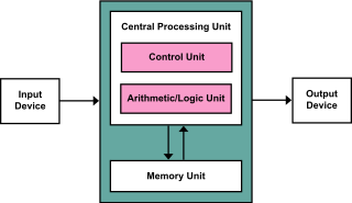
The von Neumann architecture—also known as the von Neumann model or Princeton architecture—is a computer architecture based on a 1945 description by John von Neumann, and by others, in the First Draft of a Report on the EDVAC. The document describes a design architecture for an electronic digital computer with these components:

A processor register is a quickly accessible location available to a computer's processor. Registers usually consist of a small amount of fast storage, although some registers have specific hardware functions, and may be read-only or write-only. In computer architecture, registers are typically addressed by mechanisms other than main memory, but may in some cases be assigned a memory address e.g. DEC PDP-10, ICT 1900.

<span class="mw-page-title-main">Memory address</span> Reference to a specific memory location

In computing, a memory address is a reference to a specific memory location used at various levels by software and hardware. Memory addresses are fixed-length sequences of digits conventionally displayed and manipulated as unsigned integers. Such numerical semantic bases itself upon features of CPU, as well upon use of the memory like an array endorsed by various programming languages.

A CPU cache is a hardware cache used by the central processing unit (CPU) of a computer to reduce the average cost to access data from the main memory. A cache is a smaller, faster memory, located closer to a processor core, which stores copies of the data from frequently used main memory locations. Most CPUs have a hierarchy of multiple cache levels, with different instruction-specific and data-specific caches at level 1. The cache memory is typically implemented with static random-access memory (SRAM), in modern CPUs by far the largest part of them by chip area, but SRAM is not always used for all levels, or even any level, sometimes some latter or all levels are implemented with eDRAM.

A von Neumann language in computing is a programming language that is a high-level abstract isomorphic copy of a von Neumann architecture. As of 2009, most current programming languages fit into this description, likely as a consequence of the extensive domination of the von Neumann computer architecture during the past 50 years.

<span class="mw-page-title-main">Microarchitecture</span> Component of computer engineering

In electronics, computer science and computer engineering, microarchitecture, also called computer organization and sometimes abbreviated as µarch or uarch, is the way a given instruction set architecture (ISA) is implemented in a particular processor. A given ISA may be implemented with different microarchitectures; implementations may vary due to different goals of a given design or due to shifts in technology.

The Atmel AVR instruction set is the machine language for the Atmel AVR, a modified Harvard architecture 8-bit RISC single chip microcontroller which was developed by Atmel in 1996. The AVR was one of the first microcontroller families to use on-chip flash memory for program storage.

<span class="mw-page-title-main">Hardware acceleration</span> Specialized computer hardware

Hardware acceleration is the use of computer hardware designed to perform specific functions more efficiently when compared to software running on a general-purpose central processing unit (CPU). Any transformation of data that can be calculated in software running on a generic CPU can also be calculated in custom-made hardware, or in some mix of both.

ARM9 is a group of 32-bit RISC ARM processor cores licensed by ARM Holdings for microcontroller use. The ARM9 core family consists of ARM9TDMI, ARM940T, ARM9E-S, ARM966E-S, ARM920T, ARM922T, ARM946E-S, ARM9EJ-S, ARM926EJ-S, ARM968E-S, ARM996HS. Since ARM9 cores were released from 1998 to 2006, they are no longer recommended for new IC designs, instead ARM Cortex-A, ARM Cortex-M, ARM Cortex-R cores are preferred.

Memory architecture describes the methods used to implement electronic computer data storage in a manner that is a combination of the fastest, most reliable, most durable, and least expensive way to store and retrieve information. Depending on the specific application, a compromise of one of these requirements may be necessary in order to improve another requirement. Memory architecture also explains how binary digits are converted into electric signals and then stored in the memory cells. And also the structure of a memory cell.

This glossary of computer hardware terms is a list of definitions of terms and concepts related to computer hardware, i.e. the physical and structural components of computers, architectural issues, and peripheral devices.

References

  1. A Manual of Operation for the Automatic Sequence Controlled Calculator. OXFORD UNIVERSITY PRESS. p. 4.
  2. "AVR109: Self Programming" (PDF) (Application note). Atmel. June 2004. Retrieved 29 January 2015.
  3. "MAXQ Family User's Guide". Maxim Integrated. September 2008. Sections 1.2 "Harvard Memory Architecture" and 2.5 "Pseudo-Von Neumann Memory Access".
  4. Konark Goel et al. About MAXQ GCC port.