
MEMS is the technology of microscopic devices incorporating both electronic and moving parts. MEMS are made up of components between 1 and 100 micrometres in size, and MEMS devices generally range in size from 20 micrometres to a millimetre, although components arranged in arrays can be more than 1000 mm2. They usually consist of a central unit that processes data and several components that interact with the surroundings.

A corona discharge is an electrical discharge caused by the ionization of a fluid such as air surrounding a conductor carrying a high voltage. It represents a local region where the air has undergone electrical breakdown and become conductive, allowing charge to continuously leak off the conductor into the air. A corona discharge occurs at locations where the strength of the electric field around a conductor exceeds the dielectric strength of the air. It is often seen as a bluish glow in the air adjacent to pointed metal conductors carrying high voltages, and emits light by the same mechanism as a gas discharge lamp, chemiluminescence. Corona discharges can also happen in weather, such as thunderstorms, where objects like ship masts or airplane wings have a charge significantly different from the air around them.

Corona treatment is a surface modification technique that uses a low temperature corona discharge plasma to impart changes in the properties of a surface. The corona plasma is generated by the application of high voltage to an electrode that has a sharp tip. The plasma forms at the tip. A linear array of electrodes is often used to create a curtain of corona plasma. Materials such as plastics, cloth, or paper may be passed through the corona plasma curtain in order to change the surface energy of the material. All materials have an inherent surface energy. Surface treatment systems are available for virtually any surface format including dimensional objects, sheets and roll goods that are handled in a web format. Corona treatment is a widely used surface treatment method in the plastic film, extrusion, and converting industries.
Plasma etching is a form of plasma processing used to fabricate integrated circuits. It involves a high-speed stream of glow discharge (plasma) of an appropriate gas mixture being shot at a sample. The plasma source, known as etch species, can be either charged (ions) or neutral. During the process, the plasma generates volatile etch products at room temperature from the chemical reactions between the elements of the material etched and the reactive species generated by the plasma. Eventually the atoms of the shot element embed themselves at or just below the surface of the target, thus modifying the physical properties of the target.
Plasma activation is a method of surface modification employing plasma processing, which improves surface adhesion properties of many materials including metals, glass, ceramics, a broad range of polymers and textiles and even natural materials such as wood and seeds. Plasma functionalization also refers to the introduction of functional groups on the surface of exposed materials. It is widely used in industrial processes to prepare surfaces for bonding, gluing, coating and painting. Plasma processing achieves this effect through a combination of reduction of metal oxides, ultra-fine surface cleaning from organic contaminants, modification of the surface topography and deposition of functional chemical groups. Importantly, the plasma activation can be performed at atmospheric pressure using air or typical industrial gases including hydrogen, nitrogen and oxygen. Thus, the surface functionalization is achieved without expensive vacuum equipment or wet chemistry, which positively affects its costs, safety and environmental impact. Fast processing speeds further facilitate numerous industrial applications.

Plasma-enhanced chemical vapor deposition (PECVD) is a chemical vapor deposition process used to deposit thin films from a gas state (vapor) to a solid state on a substrate. Chemical reactions are involved in the process, which occur after creation of a plasma of the reacting gases. The plasma is generally created by radio frequency (RF) alternating current (AC) frequency or direct current (DC) discharge between two electrodes, the space between which is filled with the reacting gases.
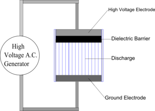
Dielectric-barrier discharge (DBD) is the electrical discharge between two electrodes separated by an insulating dielectric barrier. Originally called silent (inaudible) discharge and also known as ozone production discharge or partial discharge, it was first reported by Ernst Werner von Siemens in 1857.
Adhesive bonding describes a wafer bonding technique with applying an intermediate layer to connect substrates of different types of materials. Those connections produced can be soluble or insoluble.
A microplasma is a plasma of small dimensions, ranging from tens to thousands of micrometers. Microplasmas can be generated at a variety of temperatures and pressures, existing as either thermal or non-thermal plasmas. Non-thermal microplasmas that can maintain their state at standard temperatures and pressures are readily available and accessible to scientists as they can be easily sustained and manipulated under standard conditions. Therefore, they can be employed for commercial, industrial, and medical applications, giving rise to the evolving field of microplasmas.

Atmospheric-pressure plasma is a plasma in which the pressure approximately matches that of the surrounding atmosphere – the so-called normal pressure.
Plasma medicine is an emerging field that combines plasma physics, life sciences and clinical medicine. It is being studied in disinfection, healing, cancer, and surgery. Most of the research is in vitro and in animal models.
Ultra-high-purity steam, also called the clean steam, UHP steam or high purity water vapor, is used in a variety of industrial manufacturing processes that require oxidation or annealing. These processes include the growth of oxide layers on silicon wafers for the semiconductor industry, originally described by the Deal-Grove model, and for the formation of passivation layers used to improve the light capture ability of crystalline photovoltaic cells. Several methods and technologies can be employed to generate ultra high purity steam, including pyrolysis, bubbling, direct liquid injection, and purified steam generation. The level of purity, or the relative lack of contamination, affects the quality of the oxide layer or annealed surface. The method of delivery affects growth rate, uniformity, and electrical performance. Oxidation and annealing are common steps in the manufacture of such devices as microelectronics and solar cells.
Direct bonding, or fusion bonding, is a wafer bonding process without any additional intermediate layers. It is based on chemical bonds between two surfaces of any material possible meeting numerous requirements. These requirements are specified for the wafer surface as sufficiently clean, flat and smooth. Otherwise unbonded areas so called voids, i.e. interface bubbles, can occur.
Anodic bonding is a wafer bonding process to seal glass to either silicon or metal without introducing an intermediate layer. Anodic bonding is commonly used to seal glass to silicon wafers in electronics and microfluidics. Anodic bonding, also known as field assisted bonding or electrostatic sealing, is mostly used for connecting silicon/glass and metal/glass through electric fields. The requirements for anodic bonding are clean and even wafer surfaces and atomic contact between the bonding substrates through a sufficiently powerful electrostatic field. Also necessary is the use of borosilicate glass containing a high concentration of alkali ions. The coefficient of thermal expansion (CTE) of the processed glass needs to be similar to those of the bonding partner.
Wafer bonding is a packaging technology on wafer-level for the fabrication of microelectromechanical systems (MEMS), nanoelectromechanical systems (NEMS), microelectronics and optoelectronics, ensuring a mechanically stable and hermetically sealed encapsulation. The wafers' diameter range from 100 mm to 200 mm for MEMS/NEMS and up to 300 mm for the production of microelectronic devices. Smaller wafers were used in the early days of the microelectronics industry, with wafers being just 1 inch in diameter in the 1950s.
Eutectic bonding, also referred to as eutectic soldering, describes a wafer bonding technique with an intermediate metal layer that can produce a eutectic system. Those eutectic metals are alloys that transform directly from solid to liquid state, or vice versa from liquid to solid state, at a specific composition and temperature without passing a two-phase equilibrium, i.e. liquid and solid state. The fact that the eutectic temperature can be much lower than the melting temperature of the two or more pure elements can be important in eutectic bonding.
Glass frit bonding, also referred to as glass soldering or seal glass bonding, describes a wafer bonding technique with an intermediate glass layer. It is a widely used encapsulation technology for surface micro-machined structures, e.g., accelerometers or gyroscopes. The technique utilizes low melting-point glass and therefore provides various advantages including that viscosity of glass decreases with an increase of temperature. The viscous flow of glass has effects to compensate and planarize surface irregularities, convenient for bonding wafers with a high roughness due to plasma etching or deposition. A low viscosity promotes hermetically sealed encapsulation of structures based on a better adaption of the structured shapes. Further, the coefficient of thermal expansion (CTE) of the glass material is adapted to silicon. This results in low stress in the bonded wafer pair. The glass has to flow and wet the soldered surfaces well below the temperature where deformation or degradation of either of the joined materials or nearby structures occurs. The usual temperature of achieving flowing and wetting is between 450 and 550 °C.
Reactive bonding is a wafer bonding procedure that uses highly reactive nanoscale multilayer systems as an intermediate layer between the bonding substrates. The multilayer system consists of two alternating different thin metallic films. The self-propagating exothermic reaction within the multilayer system contributes the local heat to bond the solder films. Based on the limited temperature the substrate material is exposed, temperature-sensitive components and materials with different CTEs, i.e. metals, polymers and ceramics, can be used without thermal damage.
An excimer lamp is a source of ultraviolet light based on spontaneous emission of excimer (exciplex) molecules.
Piezoelectric direct discharge (PDD) plasma is a type of cold non-equilibrium plasma, generated by a direct gas discharge of a high voltage piezoelectric transformer. It can be ignited in air or other gases in a wide range of pressures, including atmospheric. Due to the compactness and the efficiency of the piezoelectric transformer, this method of plasma generation is particularly compact, efficient and cheap. It enables a wide spectrum of industrial, medical and consumer applications.


