
A remote plasma (also downstream plasma or afterglow plasma) is a plasma processing method in which the plasma and material interaction occurs at a location remote from the plasma in the plasma afterglow. [1] [2]
A remote plasma (also downstream plasma or afterglow plasma) is a plasma processing method in which the plasma and material interaction occurs at a location remote from the plasma in the plasma afterglow. [1] [2]

Chemical vapor deposition (CVD) is a vacuum deposition method used to produce high-quality, and high-performance, solid materials. The process is often used in the semiconductor industry to produce thin films.
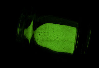
A phosphor is a substance that exhibits the phenomenon of luminescence; it emits light when exposed to some type of radiant energy. The term is used both for fluorescent or phosphorescent substances which glow on exposure to ultraviolet or visible light, and cathodoluminescent substances which glow when struck by an electron beam in a cathode-ray tube.
In chemistry, deposition occurs when molecules settle out of a solution.
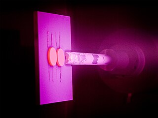
A plasma afterglow is the radiation emitted from a plasma after the source of ionization is removed. The external electromagnetic fields that sustained the plasma glow are absent or insufficient to maintain the discharge in the afterglow. A plasma afterglow can either be a temporal, due to an interrupted (pulsed) plasma source, or spatial, due to a distant plasma source. In the afterglow, plasma-generated species de-excite and participate in secondary chemical reactions that tend to form stable species. Depending on the gas composition, super-elastic collisions may continue to sustain the plasma in the afterglow for a while by releasing the energy stored in rovibronic degrees of freedom of the atoms and molecules of the plasma. Especially in molecular gases, the plasma chemistry in the afterglow is significantly different from the plasma glow. The afterglow of a plasma is still a plasma and as thus retains most of the properties of a plasma.
Plasma processing is a plasma-based material processing technology that aims at modifying the chemical and physical properties of a surface.

Tungsten(VI) fluoride, also known as tungsten hexafluoride, is an inorganic compound with the formula WF6. It is a toxic, corrosive, colorless gas, with a density of about 13 kg/m3 (22 lb/cu yd). It is one of the densest known gases under standard conditions. WF6 ls commonly used by the semiconductor industry to form tungsten films, through the process of chemical vapor deposition. This layer is used in a low-resistivity metallic "interconnect". It is one of seventeen known binary hexafluorides.
A thin film is a layer of material ranging from fractions of a nanometer (monolayer) to several micrometers in thickness. The controlled synthesis of materials as thin films is a fundamental step in many applications. A familiar example is the household mirror, which typically has a thin metal coating on the back of a sheet of glass to form a reflective interface. The process of silvering was once commonly used to produce mirrors, while more recently the metal layer is deposited using techniques such as sputtering. Advances in thin film deposition techniques during the 20th century have enabled a wide range of technological breakthroughs in areas such as magnetic recording media, electronic semiconductor devices, integrated passive devices, LEDs, optical coatings, hard coatings on cutting tools, and for both energy generation and storage. It is also being applied to pharmaceuticals, via thin-film drug delivery. A stack of thin films is called a multilayer.

Metallizing is the general name for the technique of coating metal on the surface of objects. Metallic coatings may be decorative, protective or functional.

Flowing-afterglow mass spectrometry (FA-MS), is an analytical chemistry technique for the sensitive detection of trace gases. Trace gas molecules are ionized by the production and flow of thermalized hydrated hydronium cluster ions in a plasma afterglow of helium or argon carrier gas along a flow tube following the introduction of a humid air sample. These ions react in multiple collisions with water molecules, their isotopic compositions reach equilibrium and the relative magnitudes of their isotopomers are measured by mass spectrometry.

Ion plating (IP) is a physical vapor deposition (PVD) process that is sometimes called ion assisted deposition (IAD) or ion vapor deposition (IVD) and is a modified version of vacuum deposition. Ion plating uses concurrent or periodic bombardment of the substrate, and deposits film by atomic-sized energetic particles called ions. Bombardment prior to deposition is used to sputter clean the substrate surface. During deposition the bombardment is used to modify and control the properties of the depositing film. It is important that the bombardment be continuous between the cleaning and the deposition portions of the process to maintain an atomically clean interface. If this interface is not properly cleaned, then it can result into a weaker coating or poor adhesion.
Atomic layer deposition (ALD) is a thin-film deposition technique based on the sequential use of a gas-phase chemical process; it is a subclass of chemical vapour deposition. The majority of ALD reactions use two chemicals called precursors. These precursors react with the surface of a material one at a time in a sequential, self-limiting, manner. A thin film is slowly deposited through repeated exposure to separate precursors. ALD is a key process in fabricating semiconductor devices, and part of the set of tools for synthesizing nanomaterials.
Vacuum deposition is a group of processes used to deposit layers of material atom-by-atom or molecule-by-molecule on a solid surface. These processes operate at pressures well below atmospheric pressure. The deposited layers can range from a thickness of one atom up to millimeters, forming freestanding structures. Multiple layers of different materials can be used, for example to form optical coatings. The process can be qualified based on the vapor source; physical vapor deposition uses a liquid or solid source and chemical vapor deposition uses a chemical vapor.
Physical vapor deposition (PVD), sometimes called physical vapor transport (PVT), describes a variety of vacuum deposition methods which can be used to produce thin films and coatings on substrates including metals, ceramics, glass, and polymers. PVD is characterized by a process in which the material transitions from a condensed phase to a vapor phase and then back to a thin film condensed phase. The most common PVD processes are sputtering and evaporation. PVD is used in the manufacturing of items which require thin films for optical, mechanical, electrical, acoustic or chemical functions. Examples include semiconductor devices such as thin-film solar cells, microelectromechanical devices such as thin film bulk acoustic resonator, aluminized PET film for food packaging and balloons, and titanium nitride coated cutting tools for metalworking. Besides PVD tools for fabrication, special smaller tools used mainly for scientific purposes have been developed.
Bis(trimethylsilyl)amine (also known as hexamethyldisilazane and HMDS) is an organosilicon compound with the molecular formula [(CH3)3Si]2NH. The molecule is a derivative of ammonia with trimethylsilyl groups in place of two hydrogen atoms. An electron diffraction study shows that silicon-nitrogen bond length (173.5 pm) and Si-N-Si bond angle (125.5°) to be similar to disilazane (in which methyl groups are replaced by hydrogen atoms) suggesting that steric factors are not a factor in regulating angles in this case. This colorless liquid is a reagent and a precursor to bases that are popular in organic synthesis and organometallic chemistry. Additionally, HMDS is also increasingly used as molecular precursor in chemical vapor deposition techniques to deposit silicon carbonitride thin films or coatings.

Plasma-enhanced chemical vapor deposition (PECVD) is a chemical vapor deposition process used to deposit thin films from a gas state (vapor) to a solid state on a substrate. Chemical reactions are involved in the process, which occur after creation of a plasma of the reacting gases. The plasma is generally created by radio frequency (RF) frequency or direct current (DC) discharge between two electrodes, the space between which is filled with the reacting gases.

Plasma-immersion ion implantation (PIII) or pulsed-plasma doping is a surface modification technique of extracting the accelerated ions from the plasma by applying a high voltage pulsed DC or pure DC power supply and targeting them into a suitable substrate or electrode with a semiconductor wafer placed over it, so as to implant it with suitable dopants. The electrode is a cathode for an electropositive plasma, while it is an anode for an electronegative plasma. Plasma can be generated in a suitably designed vacuum chamber with the help of various plasma sources such as electron cyclotron resonance plasma source which yields plasma with the highest ion density and lowest contamination level, helicon plasma source, capacitively coupled plasma source, inductively coupled plasma source, DC glow discharge and metal vapor arc. The vacuum chamber can be of two types - diode and triode type depending upon whether the power supply is applied to the substrate as in the former case or to the perforated grid as in the latter.

The vapor–liquid–solid method (VLS) is a mechanism for the growth of one-dimensional structures, such as nanowires, from chemical vapor deposition. The growth of a crystal through direct adsorption of a gas phase on to a solid surface is generally very slow. The VLS mechanism circumvents this by introducing a catalytic liquid alloy phase which can rapidly adsorb a vapor to supersaturation levels, and from which crystal growth can subsequently occur from nucleated seeds at the liquid–solid interface. The physical characteristics of nanowires grown in this manner depend, in a controllable way, upon the size and physical properties of the liquid alloy.
Silanization of silicon and mica is the coating of these materials with a thin layer of self assembling units.
The surface chemistry of paper is responsible for many important paper properties, such as gloss, waterproofing, and printability. Many components are used in the paper-making process that affect the surface.
Nanolamination is the production of materials that are fully dense, ultra-fine grained solids that exhibit a high concentration of interface defects. The properties of fabricated nanolaminates depend on their compositions and thicknesses.
| | This article about materials science is a stub. You can help Wikipedia by expanding it. |