
In microelectronics, a dual in-line package is an electronic component package with a rectangular housing and two parallel rows of electrical connecting pins. The package may be through-hole mounted to a printed circuit board (PCB) or inserted in a socket. The dual-inline format was invented by Don Forbes, Rex Rice and Bryant Rogers at Fairchild R&D in 1964, when the restricted number of leads available on circular transistor-style packages became a limitation in the use of integrated circuits. Increasingly complex circuits required more signal and power supply leads ; eventually microprocessors and similar complex devices required more leads than could be put on a DIP package, leading to development of higher-density chip carriers. Furthermore, square and rectangular packages made it easier to route printed-circuit traces beneath the packages.

A printed circuit board (PCB), also called printed wiring board (PWB), is a laminated sandwich structure of conductive and insulating layers, each with a pattern of traces, planes and other features etched from one or more sheet layers of copper laminated onto or between sheet layers of a non-conductive substrate. PCBs are used to connect or "wire" components to one another in an electronic circuit. Electrical components may be fixed to conductive pads on the outer layers, generally by soldering, which both electrically connects and mechanically fastens the components to the board. Another manufacturing process adds vias, metal-lined drilled holes that enable electrical interconnections between conductive layers, to boards with more than a single side.
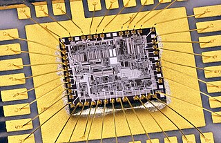
Wire bonding is a method of making interconnections between an integrated circuit (IC) or other semiconductor device and its packaging during semiconductor device fabrication. Wire bonding can also be used to connect an IC to other electronics or to connect from one printed circuit board (PCB) to another, although these are less common. Wire bonding is generally considered the most cost-effective and flexible interconnect technology and is used to assemble the vast majority of semiconductor packages. Wire bonding can be used at frequencies above 100 GHz.

A ball grid array (BGA) is a type of surface-mount packaging used for integrated circuits. BGA packages are used to permanently mount devices such as microprocessors. A BGA can provide more interconnection pins than can be put on a dual in-line or flat package. The whole bottom surface of the device can be used, instead of just the perimeter. The traces connecting the package's leads to the wires or balls which connect the die to package are also on average shorter than with a perimeter-only type, leading to better performance at high speeds.

Flip chip, also known as controlled collapse chip connection or its abbreviation, C4, is a method for interconnecting dies such as semiconductor devices, IC chips, integrated passive devices and microelectromechanical systems (MEMS), to external circuitry with solder bumps that have been deposited onto the chip pads. The technique was developed by General Electric's Light Military Electronics Department, Utica, New York. The solder bumps are deposited on the chip pads on the top side of the wafer during the final wafer processing step. In order to mount the chip to external circuitry, it is flipped over so that its top side faces down, and aligned so that its pads align with matching pads on the external circuit, and then the solder is reflowed to complete the interconnect. This is in contrast to wire bonding, in which the chip is mounted upright and fine wires are welded onto the chip pads and lead frame contacts to interconnect the chip pads to external circuitry.

Integrated circuit packaging is the final stage of semiconductor device fabrication, in which the die is encapsulated in a supporting case that prevents physical damage and corrosion. The case, known as a "package", supports the electrical contacts which connect the device to a circuit board.
A quad flat package (QFP) is a surface-mounted integrated circuit package with "gull wing" leads extending from each of the four sides. Socketing such packages is rare and through-hole mounting is not possible. Versions ranging from 32 to 304 pins with a pitch ranging from 0.4 to 1.0 mm are common. Other special variants include low-profile QFP (LQFP) and thin QFP (TQFP).
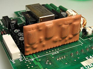
A hybrid integrated circuit (HIC), hybrid microcircuit, hybrid circuit or simply hybrid is a miniaturized electronic circuit constructed of individual devices, such as semiconductor devices and passive components, bonded to a substrate or printed circuit board (PCB). A PCB having components on a Printed wiring board (PWB) is not considered a true hybrid circuit according to the definition of MIL-PRF-38534.

Flat no-leads packages such as quad-flat no-leads (QFN) and dual-flat no-leads (DFN) physically and electrically connect integrated circuits to printed circuit boards. Flat no-leads, also known as micro leadframe (MLF) and SON, is a surface-mount technology, one of several package technologies that connect ICs to the surfaces of PCBs without through-holes. Flat no-lead is a near chip scale plastic encapsulated package made with a planar copper lead frame substrate. Perimeter lands on the package bottom provide electrical connections to the PCB. Flat no-lead packages usually, but not always, include an exposed thermally conductive pad to improve heat transfer out of the IC. Heat transfer can be further facilitated by metal vias in the thermal pad. The QFN package is similar to the quad-flat package (QFP), and a ball grid array (BGA).
Package on a package (PoP) is an integrated circuit packaging method to vertically combine discrete logic and memory ball grid array (BGA) packages. Two or more packages are installed atop each other, i.e. stacked, with a standard interface to route signals between them. This allows higher component density in devices, such as mobile phones, personal digital assistants (PDA), and digital cameras, at the cost of slightly higher height requirements. Stacks with more than 2 packages are uncommon, due to heat dissipation considerations.
A three-dimensional integrated circuit is a MOS integrated circuit (IC) manufactured by stacking as many as 16 or more ICs and interconnecting them vertically using, for instance, through-silicon vias (TSVs) or Cu-Cu connections, so that they behave as a single device to achieve performance improvements at reduced power and smaller footprint than conventional two dimensional processes. The 3D IC is one of several 3D integration schemes that exploit the z-direction to achieve electrical performance benefits in microelectronics and nanoelectronics.

The thermal copper pillar bump, also known as the "thermal bump", is a thermoelectric device made from thin-film thermoelectric material embedded in flip chip interconnects for use in electronics and optoelectronic packaging, including: flip chip packaging of CPU and GPU integrated circuits (chips), laser diodes, and semiconductor optical amplifiers (SOA). Unlike conventional solder bumps that provide an electrical path and a mechanical connection to the package, thermal bumps act as solid-state heat pumps and add thermal management functionality locally on the surface of a chip or to another electrical component. The diameter of a thermal bump is 238 μm and 60 μm high.

Integrated passive devices (IPDs), also known as integrated passive components (IPCs) or embedded passive components (EPC), are electronic components where resistors (R), capacitors (C), inductors (L)/coils/chokes, microstriplines, impedance matching elements, baluns or any combinations of them are integrated in the same package or on the same substrate. Sometimes integrated passives can also be called as embedded passives, and still the difference between integrated and embedded passives is technically unclear. In both cases passives are realized in between dielectric layers or on the same substrate.

BPDA or biphenyl-tetracarboxylic acid dianhydride is a monomer used in the production of some polyimides.
A semiconductor package is a metal, plastic, glass, or ceramic casing containing one or more discrete semiconductor devices or integrated circuits. Individual components are fabricated on semiconductor wafers before being diced into die, tested, and packaged. The package provides a means for connecting it to the external environment, such as printed circuit board, via leads such as lands, balls, or pins; and protection against threats such as mechanical impact, chemical contamination, and light exposure. Additionally, it helps dissipate heat produced by the device, with or without the aid of a heat spreader. There are thousands of package types in use. Some are defined by international, national, or industry standards, while others are particular to an individual manufacturer.
Thermosonic bonding is widely used to wire bond silicon integrated circuits into computers. Alexander Coucoulas was named "Father of Thermosonic Bonding" by George Harman, the world's foremost authority on wire bonding, where he referenced Coucoulas's leading edge publications in his book, Wire Bonding In Microelectronics. Owing to the well proven reliability of thermosonic bonds, it is extensively used to connect the central processing units (CPUs), which are encapsulated silicon integrated circuits that serve as the "brains" of today's computers.

Alexander Coucoulas is an American inventor, research engineer, and author. He was named "father of thermosonic bonding" by George Harman, the world's foremost authority on wire bonding, where he referenced Coucoulas's leading edge publications in his book, Wire Bonding In Microelectronics. A thermosonic bond is formed using a set of parameters which include ultrasonic, thermal and mechanical (force) energies.

Chip on board (COB) is a method of circuit board manufacturing in which the integrated circuits (e.g. microprocessors) are attached (wired, bonded directly) to a printed circuit board, and covered by a blob of epoxy. Chip on board eliminates the packaging of individual semiconductor devices, which allows a completed product to be less costly, lighter, and more compact. In some cases, COB construction improves the operation of radio frequency systems by reducing the inductance and capacitance of integrated circuit leads.
Glossary of microelectronics manufacturing terms


