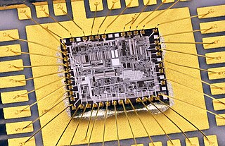
Wire bonding is a method of making interconnections between an integrated circuit (IC) or other semiconductor device and its packaging during semiconductor device fabrication. Wire bonding can also be used to connect an IC to other electronics or to connect from one printed circuit board (PCB) to another, although these are less common. Wire bonding is generally considered the most cost-effective and flexible interconnect technology and is used to assemble the vast majority of semiconductor packages. Wire bonding can be used at frequencies above 100 GHz.
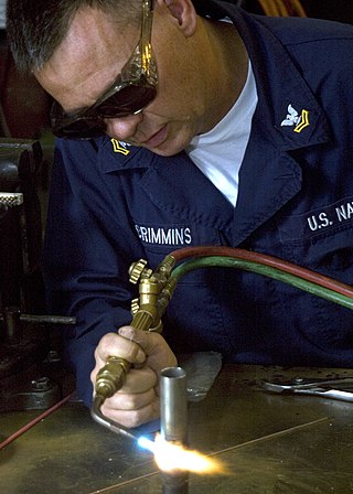
Brazing is a metal-joining process in which two or more metal items are joined by melting and flowing a filler metal into the joint, with the filler metal having a lower melting point than the adjoining metal.

Ultrasonic welding is an industrial process whereby high-frequency ultrasonic acoustic vibrations are locally applied to work pieces being held together under pressure to create a solid-state weld. It is commonly used for plastics and metals, and especially for joining dissimilar materials. In ultrasonic welding, there are no connective bolts, nails, soldering materials, or adhesives necessary to bind the materials together. When used to join metals, the temperature stays well below the melting point of the involved materials, preventing any unwanted properties which may arise from high temperature exposure of the metal.
Electric resistance welding (ERW) is a welding process in which metal parts in contact are permanently joined by heating them with an electric current, melting the metal at the joint. Electric resistance welding is widely used, for example, in manufacture of steel pipe and in assembly of bodies for automobiles. The electric current can be supplied to electrodes that also apply clamping pressure, or may be induced by an external magnetic field. The electric resistance welding process can be further classified by the geometry of the weld and the method of applying pressure to the joint: spot welding, seam welding, flash welding, projection welding, for example. Some factors influencing heat or welding temperatures are the proportions of the workpieces, the metal coating or the lack of coating, the electrode materials, electrode geometry, electrode pressing force, electric current and length of welding time. Small pools of molten metal are formed at the point of most electrical resistance as an electric current is passed through the metal. In general, resistance welding methods are efficient and cause little pollution, but their applications are limited to relatively thin materials.

A piezoelectric motor or piezo motor is a type of electric motor based on the change in shape of a piezoelectric material when an electric field is applied, as a consequence of the converse piezoelectric effect. An electrical circuit makes acoustic or ultrasonic vibrations in the piezoelectric material, most often lead zirconate titanate and occasionally lithium niobate or other single-crystal materials, which can produce linear or rotary motion depending on their mechanism. Examples of types of piezoelectric motors include inchworm motors, stepper and slip-stick motors as well as ultrasonic motors which can be further categorized into standing wave and travelling wave motors. Piezoelectric motors typically use a cyclic stepping motion, which allows the oscillation of the crystals to produce an arbitrarily large motion, as opposed to most other piezoelectric actuators where the range of motion is limited by the static strain that may be induced in the piezoelectric element.
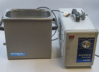
Ultrasonic cleaning is a process that uses ultrasound to agitate a fluid, with a cleaning effect. Ultrasonic cleaners come in a variety of sizes, from small desktop units with an internal volume of less than 0.5 litres (0.13 US gal), to large industrial units with volumes approaching 1,000 litres.
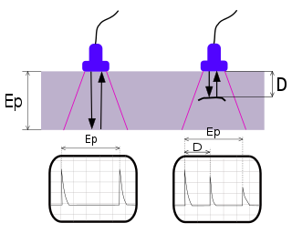
Ultrasonic testing (UT) is a family of non-destructive testing techniques based on the propagation of ultrasonic waves in the object or material tested. In most common UT applications, very short ultrasonic pulse waves with centre frequencies ranging from 0.1-15 MHz and occasionally up to 50 MHz, are transmitted into materials to detect internal flaws or to characterize materials. A common example is ultrasonic thickness measurement, which tests the thickness of the test object, for example, to monitor pipework corrosion and erosion. Ultrasonic testing is extensively used to detect flaws in welds.

Flat no-leads packages such as quad-flat no-leads (QFN) and dual-flat no-leads (DFN) physically and electrically connect integrated circuits to printed circuit boards. Flat no-leads, also known as micro leadframe (MLF) and SON, is a surface-mount technology, one of several package technologies that connect ICs to the surfaces of PCBs without through-holes. Flat no-lead is a near chip scale plastic encapsulated package made with a planar copper lead frame substrate. Perimeter lands on the package bottom provide electrical connections to the PCB. Flat no-lead packages usually, but not always, include an exposed thermally conductive pad to improve heat transfer out of the IC. Heat transfer can be further facilitated by metal vias in the thermal pad. The QFN package is similar to the quad-flat package (QFP), and a ball grid array (BGA).

Ultrasonic transducers and ultrasonic sensors are devices that generate or sense ultrasound energy. They can be divided into three broad categories: transmitters, receivers and transceivers. Transmitters convert electrical signals into ultrasound, receivers convert ultrasound into electrical signals, and transceivers can both transmit and receive ultrasound.

Electromagnetic acoustic transducer (EMAT) is a transducer for non-contact acoustic wave generation and reception in conducting materials. Its effect is based on electromagnetic mechanisms, which do not need direct coupling with the surface of the material. Due to this couplant-free feature, EMATs are particularly useful in harsh, i.e., hot, cold, clean, or dry environments. EMATs are suitable to generate all kinds of waves in metallic and/or magnetostrictive materials. Depending on the design and orientation of coils and magnets, shear horizontal (SH) bulk wave mode, surface wave, plate waves such as SH and Lamb waves, and all sorts of other bulk and guided-wave modes can be excited. After decades of research and development, EMAT has found its applications in many industries such as primary metal manufacturing and processing, automotive, railroad, pipeline, boiler and pressure vessel industries, in which they are typically used for nondestructive testing (NDT) of metallic structures.

A piezoelectric accelerometer is an accelerometer that employs the piezoelectric effect of certain materials to measure dynamic changes in mechanical variables.

An ultrasonic horn is a tapering metal bar commonly used for augmenting the oscillation displacement amplitude provided by an ultrasonic transducer operating at the low end of the ultrasonic frequency spectrum. The device is necessary because the amplitudes provided by the transducers themselves are insufficient for most practical applications of power ultrasound. Another function of the ultrasonic horn is to efficiently transfer the acoustic energy from the ultrasonic transducer into the treated media, which may be solid or liquid. Ultrasonic processing of liquids relies of intense shear forces and extreme local conditions generated by acoustic cavitation.
Ultrasonic soldering is a flux-less soldering process that uses ultrasonic energy, without the need for chemicals to solder materials, such as glass, ceramics, and composites, hard to solder metals and other sensitive components which cannot be soldered using conventional means.

Ultrasonic machining is a subtractive manufacturing process that removes material from the surface of a part through high frequency, low amplitude vibrations of a tool against the material surface in the presence of fine abrasive particles. The tool travels vertically or orthogonal to the surface of the part at amplitudes of 0.05 to 0.125 mm. The fine abrasive grains are mixed with water to form a slurry that is distributed across the part and the tip of the tool. Typical grain sizes of the abrasive material range from 100 to 1000, where smaller grains produce smoother surface finishes.
In ultrasonic machining, welding and mixing, a sonotrode is a tool that creates ultrasonic vibrations and applies this vibrational energy to a gas, liquid, solid or tissue.

Ultrasonic Consolidation (UC) or Ultrasonic Additive Manufacturing (UAM) is a low temperature additive manufacturing or 3D printing technique for metals.
Hot plate welding, also called heated tool welding, is a thermal welding technique for joining thermoplastics. A heated tool is placed against or near the two surfaces to be joined in order to melt them. Then, the heat source is removed, and the surfaces are brought together under pressure. Hot plate welding has relatively long cycle times, ranging from 10 seconds to minutes, compared to vibration or ultrasonic welding. However, its simplicity and ability to produce strong joints in almost all thermoplastics make it widely used in mass production and for large structures, like large-diameter plastic pipes. Different inspection techniques are implemented in order to identify various discontinuities or cracks.
Thermosonic bonding is widely used to wire bond silicon integrated circuits into computers. Alexander Coucoulas was named "Father of Thermosonic Bonding" by George Harman, the world's foremost authority on wire bonding, where he referenced Coucoulas's leading edge publications in his book, Wire Bonding In Microelectronics. Owing to the well proven reliability of thermosonic bonds, it is extensively used to connect the central processing units (CPUs), which are encapsulated silicon integrated circuits that serve as the "brains" of today's computers.

Alexander Coucoulas is an American inventor, research engineer, and author. He was named "father of thermosonic bonding" by George Harman, the world's foremost authority on wire bonding, where he referenced Coucoulas's leading edge publications in his book, Wire Bonding In Microelectronics. A thermosonic bond is formed using a set of parameters which include ultrasonic, thermal and mechanical (force) energies.


