Multi-threshold CMOS

Last updated

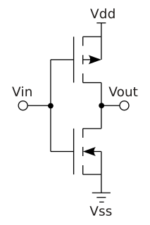
Multi-threshold CMOS (MTCMOS) is a variation of CMOS chip technology which has transistors with multiple threshold voltages (Vth) in order to optimize delay or power. The Vth of a MOSFET is the gate voltage where an inversion layer forms at the interface between the insulating layer (oxide) and the substrate (body) of the transistor. Low Vth devices switch faster, and are therefore useful on critical delay paths to minimize clock periods[ clarification needed ]. The penalty is that low Vth devices have substantially higher static leakage power. High Vth devices are used on non-critical paths to reduce static leakage power without incurring a delay penalty. Typical high Vth devices reduce static leakage by 10 times compared with low Vth devices. [1]

CMOS technology for constructing integrated circuits

Complementary metal–oxide–semiconductor (CMOS) is a technology for constructing integrated circuits. CMOS technology is used in microprocessors, microcontrollers, static RAM, and other digital logic circuits. CMOS technology is also used for several analog circuits such as image sensors, data converters, and highly integrated transceivers for many types of communication. Frank Wanlass patented CMOS in 1967 while working for Fairchild Semiconductor.

Integrated circuit electronic circuit manufactured by lithography; set of electronic circuits on one small flat piece (or "chip") of semiconductor material, normally silicon

An integrated circuit or monolithic integrated circuit is a set of electronic circuits on one small flat piece of semiconductor material that is normally silicon. The integration of large numbers of tiny transistors into a small chip results in circuits that are orders of magnitude smaller, faster, and less expensive than those constructed of discrete electronic components. The IC's mass production capability, reliability, and building-block approach to circuit design has ensured the rapid adoption of standardized ICs in place of designs using discrete transistors. ICs are now used in virtually all electronic equipment and have revolutionized the world of electronics. Computers, mobile phones, and other digital home appliances are now inextricable parts of the structure of modern societies, made possible by the small size and low cost of ICs.

Transistor semiconductor device used to amplify and switch electronic signals and electrical power

A transistor is a semiconductor device used to amplify or switch electronic signals and electrical power. It is composed of semiconductor material usually with at least three terminals for connection to an external circuit. A voltage or current applied to one pair of the transistor's terminals controls the current through another pair of terminals. Because the controlled (output) power can be higher than the controlling (input) power, a transistor can amplify a signal. Today, some transistors are packaged individually, but many more are found embedded in integrated circuits.

One method of creating devices with multiple threshold voltages is to apply different bias voltages (Vb) to the base or bulk terminal of the transistors. Other methods involve adjusting the gate oxide thickness, gate oxide dielectric constant (material type), or dopant concentration in the channel region beneath the gate oxide.

The gate oxide is the dielectric layer that separates the gate terminal of a MOSFET from the underlying source and drain terminals as well as the conductive channel that connects source and drain when the transistor is turned on. Gate oxide is formed by oxidizing the silicon of the channel to form a thin insulating layer of silicon dioxide. A conductive gate material is subsequently deposited over the gate oxide to form the transistor. The gate oxide serves as the dielectric layer so that the gate can sustain as high as 1 to 5 MV/cm transverse electric field in order to strongly modulate the conductance of the channel.

Dielectric electrically poorly conducting or non-conducting, non-metallic substance of which charge carriers are generally not free to move

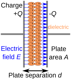
A dielectric is an electrical insulator that can be polarized by an applied electric field. When a dielectric is placed in an electric field, electric charges do not flow through the material as they do in an electrical conductor but only slightly shift from their average equilibrium positions causing dielectric polarization. Because of dielectric polarization, positive charges are displaced in the direction of the field and negative charges shift in the opposite direction. This creates an internal electric field that reduces the overall field within the dielectric itself. If a dielectric is composed of weakly bonded molecules, those molecules not only become polarized, but also reorient so that their symmetry axes align to the field.

A dopant, also called a doping agent, is a trace impurity element that is inserted into a substance to alter the electrical or optical properties of the substance. In the case of crystalline substances, the atoms of the dopant very commonly take the place of elements that were in the crystal lattice of the base material. The crystalline materials are frequently either crystals of a semiconductor such as silicon and germanium for use in solid-state electronics, or transparent crystals for use in the production of various laser types; however, in some cases of the latter, noncrystalline substances such as glass can also be doped with impurities.

A common method of fabricating multi-threshold CMOS involves simply adding additional photolithography and ion implantation steps. [2] For a given fabrication process, the Vth is adjusted by altering the concentration of dopant atoms in the channel region beneath the gate oxide. Typically, the concentration is adjusted by ion implantation method. For example, photolithography methods are applied to cover all devices except the p-MOSFETs with photoresist. Ion implantation is then completed, with ions of the chosen dopant type penetrating the gate oxide in areas where no photoresist is present. The photoresist is then stripped. Photolithography methods are again applied to cover all devices except the n-MOSFETs. Another implantation is then completed using a different dopant type, with ions penetrating the gate oxide. The photoresist is stripped. At some point during the subsequent fabrication process, implanted ions are activated by annealing at an elevated temperature.

Photolithography, also called optical lithography or UV lithography, is a process used in microfabrication to pattern parts of a thin film or the bulk of a substrate. It uses light to transfer a geometric pattern from a photomask to a photosensitive chemical photoresist on the substrate. A series of chemical treatments then either etches the exposure pattern into the material or enables deposition of a new material in the desired pattern upon the material underneath the photoresist. In complex integrated circuits, a CMOS wafer may go through the photolithographic cycle as many as 50 times.

Ion implantation Material and chemical process

Ion implantation is a low-temperature process by which ions of one element are accelerated into a solid target, thereby changing the physical, chemical, or electrical properties of the target. Ion implantation is used in semiconductor device fabrication and in metal finishing, as well as in materials science research. The ions can alter the elemental composition of the target if they stop and remain in the target. Ion implantation also causes chemical and physical changes when the ions impinge on the target at high energy. The crystal structure of the target can be damaged or even destroyed by the energetic collision cascades, and ions of sufficiently high energy can cause nuclear transmutation.

In principle, any number of threshold voltage transistors can be produced. For CMOS having two threshold voltages, one additional photomasking and implantation step is required for each of p-MOSFET and n-MOSFET. For fabrication of normal, low, and high Vth CMOS, four additional steps are required relative to conventional single-Vth CMOS.

Implementation

The most common implementation of MTCMOS for reducing power makes use of sleep transistors. Logic is supplied by a virtual power rail. Low Vth devices are used in the logic where fast switching speed is important. High Vth devices connecting the power rails and virtual power rails are turned on in active mode, off in sleep mode. High Vth devices are used as sleep transistors to reduce static leakage power.

Electric power the rate per unit of time at which electrical energy is transferred by an electric circuit

Electric power is the rate, per unit time, at which electrical energy is transferred by an electric circuit. The SI unit of power is the watt, one joule per second.

Sleep mode Low power mode for electronic devices

Sleep mode is a low power mode for electronic devices such as computers, televisions, and remote controlled devices. These modes save significantly on electrical consumption compared to leaving a device fully on and, upon resume, allow the user to avoid having to reissue instructions or to wait for a machine to reboot. Many devices signify this power mode with a pulsed or red colored LED power light.

The design of the power switch which turns on and off the power supply to the logic gates is essential to low-voltage, high-speed circuit techniques such as MTCMOS. The speed, area, and power of a logic circuit are influenced by the characteristics of the power switch.

In electrical engineering, a switch is an electrical component that can "make" or "break" an electrical circuit, interrupting the current or diverting it from one conductor to another. The mechanism of a switch removes or restores the conducting path in a circuit when it is operated. It may be operated manually, for example, a light switch or a keyboard button, may be operated by a moving object such as a door, or may be operated by some sensing element for pressure, temperature or flow. A switch will have one or more sets of contacts, which may operate simultaneously, sequentially, or alternately. Switches in high-powered circuits must operate rapidly to prevent destructive arcing, and may include special features to assist in rapidly interrupting a heavy current. Multiple forms of actuators are used for operation by hand or to sense position, level, temperature or flow. Special types are used, for example, for control of machinery, to reverse electric motors, or to sense liquid level. Many specialized forms exist. A common use is control of lighting, where multiple switches may be wired into one circuit to allow convenient control of light fixtures.

Power supply electronic device that supplies electric energy to an electrical load

A power supply is an electrical device that supplies electric power to an electrical load. The primary function of a power supply is to convert electric current from a source to the correct voltage, current, and frequency to power the load. As a result, power supplies are sometimes referred to as electric power converters. Some power supplies are separate standalone pieces of equipment, while others are built into the load appliances that they power. Examples of the latter include power supplies found in desktop computers and consumer electronics devices. Other functions that power supplies may perform include limiting the current drawn by the load to safe levels, shutting off the current in the event of an electrical fault, power conditioning to prevent electronic noise or voltage surges on the input from reaching the load, power-factor correction, and storing energy so it can continue to power the load in the event of a temporary interruption in the source power.

In electronics, a logic gate is an idealized or physical device implementing a Boolean function; that is, it performs a logical operation on one or more binary inputs and produces a single binary output. Depending on the context, the term may refer to an ideal logic gate, one that has for instance zero rise time and unlimited fan-out, or it may refer to a non-ideal physical device.

In a "coarse-grained" approach, high Vth sleep transistors gate the power to entire logic blocks. [3] The sleep signal is de-asserted during active mode, causing the transistor to turn on and provide virtual power (ground) to the low Vth logic. The sleep signal is asserted during sleep mode, causing the transistor to turn off and disconnect power (ground) from the low Vth logic. The drawbacks of this approach are that:

In a "fine-grained" approach, high Vth sleep transistors are incorporated within every gate. Low Vth transistors are used for the pull-up and pull-down networks, and a high Vth transistor is used to gate the leakage current between the two networks. This approach eliminates problems of logic block partitioning and sleep transistor sizing. However, a large amount of area overhead is added due both to inclusion of additional transistors in every Boolean gate, and in creating a sleep signal distribution tree.

An intermediate approach is to incorporate high Vth sleep transistors into threshold gates having more complicated function. Since fewer such threshold gates are required to implement any arbitrary function compared to Boolean gates, incorporating MTCMOS into each gate requires less area overhead. Examples of threshold gates having more complicated function are found with Null Convention Logic [4] and Sleep Convention Logic. [5] Some art is required to implement MTCMOS without causing glitches or other problems.

Related Research Articles

MOSFET transistor used for amplifying or switching electronic signals

The metal-oxide-semiconductor field-effect transistor is a type of field-effect transistor (FET), most commonly fabricated by the controlled oxidation of silicon. It has an insulated gate, whose voltage determines the conductivity of the device. This ability to change conductivity with the amount of applied voltage can be used for amplifying or switching electronic signals. A metal-insulator-semiconductor field-effect transistor or MISFET is a term almost synonymous with MOSFET. Another synonym is IGFET for insulated-gate field-effect transistor.

NMOS logic implements logic gates and other digital circuits

N-type metal-oxide-semiconductor logic uses n-type field-effect transistors (MOSFETs) to implement logic gates and other digital circuits. These nMOS transistors operate by creating an inversion layer in a p-type transistor body. This inversion layer, called the n-channel, can conduct electrons between n-type "source" and "drain" terminals. The n-channel is created by applying voltage to the third terminal, called the gate. Like other MOSFETs, nMOS transistors have four modes of operation: cut-off, triode, saturation, and velocity saturation.

BiCMOS is an evolved semiconductor technology that integrates two formerly separate semiconductor technologies, those of the bipolar junction transistor and the CMOS transistor, in a single integrated circuit device.

In computer engineering, a logic family may refer to one of two related concepts. A logic family of monolithic digital integrated circuit devices is a group of electronic logic gates constructed using one of several different designs, usually with compatible logic levels and power supply characteristics within a family. Many logic families were produced as individual components, each containing one or a few related basic logical functions, which could be used as "building-blocks" to create systems or as so-called "glue" to interconnect more complex integrated circuits. A "logic family" may also refer to a set of techniques used to implement logic within VLSI integrated circuits such as central processors, memories, or other complex functions. Some such logic families use static techniques to minimize design complexity. Other such logic families, such as domino logic, use clocked dynamic techniques to minimize size, power consumption and delay.

Threshold voltage Minimum source-to-gate voltage for a field effect transistor to be conducting from source to drain

The threshold voltage, commonly abbreviated as Vth, of a field-effect transistor (FET) is the minimum gate-to-source voltage VGS (th) that is needed to create a conducting path between the source and drain terminals. It is an important scaling factor to maintain power efficiency.

Subthreshold conduction

Subthreshold conduction or subthreshold leakage or subthreshold drain current is the current between the source and drain of a MOSFET when the transistor is in subthreshold region, or weak-inversion region, that is, for gate-to-source voltages below the threshold voltage. The terminology for various degrees of inversion is described in Tsividis.

The term high-κ dielectric refers to a material with a high dielectric constant κ. High-κ dielectrics are used in semiconductor manufacturing processes where they are usually used to replace a silicon dioxide gate dielectric or another dielectric layer of a device. The implementation of high-κ gate dielectrics is one of several strategies developed to allow further miniaturization of microelectronic components, colloquially referred to as extending Moore's Law.

Depletion-load NMOS logic form of nMOS logic family

In integrated circuits, depletion-load NMOS is a form of digital logic family that uses only a single power supply voltage, unlike earlier nMOS logic families that needed more than one different power supply voltage. Although manufacturing these integrated circuits required additional processing steps, improved switching speed and the elimination of the extra power supply made this logic family the preferred choice for many microprocessors and other logic elements.

Power optimization is the use of electronic design automation tools to optimize (reduce) the power consumption of a digital design, such as that of an integrated circuit, while preserving the functionality.

Shallow trench isolation integrated circuit

Shallow trench isolation (STI), also known as box isolation technique, is an integrated circuit feature which prevents electric current leakage between adjacent semiconductor device components. STI is generally used on CMOS process technology nodes of 250 nanometers and smaller. Older CMOS technologies and non-MOS technologies commonly use isolation based on LOCOS.

Negative-bias temperature instability (NBTI) is a key reliability issue in MOSFETs. NBTI manifests as an increase in the threshold voltage and consequent decrease in drain current and transconductance of a MOSFET. The degradation is often approximated by a power-law dependence on time. It is of immediate concern in p-channel MOS devices (pMOS), since they almost always operate with negative gate-to-source voltage; however, the very same mechanism also affects nMOS transistors when biased in the accumulation regime, i.e. with a negative bias applied to the gate.

In electronics, a self-aligned gate is a transistor manufacturing feature whereby a refractory gate electrode region of a MOSFET transistor is used as a mask for the doping of the source and drain regions. This technique ensures that the gate will slightly overlap the edges of the source and drain.

PMOS logic p-type MOSFETs to implement logic gates

P-type metal-oxide-semiconductor logic uses p-channel metal-oxide-semiconductor field effect transistors (MOSFETs) to implement logic gates and other digital circuits. PMOS transistors operate by creating an inversion layer in an n-type transistor body. This inversion layer, called the p-channel, can conduct holes between p-type "source" and "drain" terminals.

Dynamic voltage scaling is a power management technique in computer architecture, where the voltage used in a component is increased or decreased, depending upon circumstances. Dynamic voltage scaling to increase voltage is known as overvolting; dynamic voltage scaling to decrease voltage is known as undervolting. Undervolting is done in order to conserve power, particularly in laptops and other mobile devices, where energy comes from a battery and thus is limited, or in rare cases, to increase reliability. Overvolting is done in order to increase computer performance.

Low-power electronics are electronics, such as notebook processors, that have been designed to use less electric power.

In field effect transistors (FETs), depletion mode and enhancement mode are two major transistor types, corresponding to whether the transistor is in an ON state or an OFF state at zero gate–source voltage.

Polysilicon depletion effect is the phenomenon in which unwanted variation of threshold voltage of the MOSFET devices using polysilicon as gate material is observed, leading to unpredicted behavior of the electronic circuit. Polycrystalline silicon, also called polysilicon, is a material consisting of small silicon crystals. It differs from single-crystal silicon, used for electronics and solar cells, and from amorphous silicon, used for thin film devices and solar cells.

Field-effect transistor transistor that uses an electric field to control the electrical behaviour of the device. FETs are also known as unipolar transistors since they involve single-carrier-type operation

The field-effect transistor (FET) is an electronic device which uses an electric field to control the flow of current. FETs are 3-terminalled devices, having a source, gate, and drain terminal. FETs control the flow of current by the application of a voltage to the gate terminal, which in turn alters the conductivity between the drain and source terminals.

Advanced Linear Devices Incorporated, also known as ALD, is a semiconductor device design and manufacturing company based in Sunnyvale, California. The company develops and manufactures precision analog CMOS linear integrated circuits for industrial controls, instrumentation, computers, medical devices, automotive, and telecommunications products. It is best known for its redesign of the 555 timer IC as a low-voltage CMOS device.

References

  1. Anis, M.; Areibi; Mahmoud; Elmasry (2002). "Dynamic and leakage power reduction in MTCMOS circuits". Design Automation Conference, 2002. Proceedings. 39th: 480–485. ISBN   1-58113-461-4.
  2. Oklobdzija, Vojin G. (1997). Digital Design and Fabrication. CRC-Press. pp. 12–18. ISBN   978-0-8493-8602-2.
  3. Smith, Scott and Di, Jia (2009). Designing Asynchronous Circuits using NULL Convention Logic (NCL). Morgan & Claypool Publishers. pp. 61–73. ISBN   978-1-59829-981-6.
  4. Fant, Karl (2005). Logically Determined Design: clockless system design with NULL convention logic. John Wiley and Sons. ISBN   978-0-471-68478-7.
  5. Smith, Scott and Di, Jia. "U.S. 7,977,972" . Retrieved 2011-12-12.