Today, op amps are used widely in consumer, industrial, and scientific electronics. Many standard integrated circuit op amps cost only a few cents; however, some integrated or hybrid operational amplifiers with special performance specifications may cost over US$100.[3] Op amps may be packaged as components or used as elements of more complex integrated circuits.
An op amp without negative feedback (a comparator)
The amplifier's differential inputs consist of a non-inverting input (+) with voltage V+ and an inverting input (−) with voltage V−; ideally the op amp amplifies only the difference in voltage between the two, which is called the differential input voltage. The output voltage of the op amp Vout is given by the equation where AOL is the open-loop gain of the amplifier (the term "open-loop" refers to the absence of an external feedback loop from the output to the input).
Open-loop amplifier
The magnitude of AOL is typically very large (100,000 or more for integrated circuit op amps, corresponding to +100dB). Thus, even small microvolts of difference between V+ and V− may drive the amplifier into clipping or saturation. The magnitude of AOL is not well controlled by the manufacturing process, and so it is impractical to use an open-loop amplifier as a stand-alone differential amplifier.
Without negative feedback, and optionally positive feedback for regeneration, an open-loop op amp acts as a comparator, although comparator ICs are better suited.[4] If the inverting input of an ideal op amp is held at ground (0V), and the input voltage Vin applied to the non-inverting input is positive, the output will be maximum positive; if Vin is negative, the output will be maximum negative.
Closed-loop amplifier
An op amp with negative feedback (a non-inverting amplifier)
If predictable operation is desired, negative feedback is used, by applying a portion of the output voltage to the inverting input. The closed-loop feedback greatly reduces the gain of the circuit. When negative feedback is used, the circuit's overall gain and response is determined primarily by the feedback network, rather than by the op-amp characteristics. If the feedback network is made of components with values small relative to the op amp's input impedance, the value of the op amp's open-loop response AOL does not seriously affect the circuit's performance. In this context, high input impedance at the input terminals and low output impedance at the output terminal(s) are particularly useful features of an op amp.
The response of the op-amp circuit with its input, output, and feedback circuits to an input is characterized mathematically by a transfer function; designing an op-amp circuit to have a desired transfer function is in the realm of electrical engineering. The transfer functions are important in most applications of op amps, such as in analog computers.
In the non-inverting amplifier on the right, the presence of negative feedback via the voltage dividerRf, Rg determines the closed-loop gainACL = Vout / Vin. Equilibrium will be established when Vout is just sufficient to pull the inverting input to the same voltage as Vin. The voltage gain of the entire circuit is thus 1 + Rf / Rg. As a simple example, if Vin = 1 V and Rf = Rg, Vout will be 2V, exactly the amount required to keep V− at 1V. Because of the feedback provided by the Rf, Rg network, this is a closed-loop circuit.
Another way to analyze this circuit proceeds by making the following (usually valid) assumptions:[5]
When an op amp operates in linear (i.e., not saturated) mode, the difference in voltage between the non-inverting (+) and inverting (−) pins is negligibly small.
The input impedance of the (+) and (−) pins is much larger than other resistances in the circuit.
The input signal Vin appears at both (+) and (−) pins per assumption 1, resulting in a current i through Rg equal to Vin / Rg:
Because Kirchhoff's current law states that the same current must leave a node as enter it, and because the impedance into the (−) pin is near infinity per assumption 2, we can assume practically all of the same current i flows through Rf, creating an output voltage
By combining terms, we determine the closed-loop gain ACL:
Characteristics
Ideal op amps
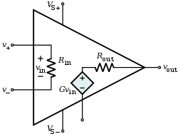
An equivalent circuit of an operational amplifier that models some resistive non-ideal parameters.
An ideal op amp is usually considered to have the following characteristics:[6][7][8]
The first rule only applies in the usual case where the op amp is used in a negative feedback design, where there is a signal path of some sort feeding back from the output to the inverting input. These rules are commonly used as a good first approximation for analyzing or designing op-amp circuits.[9]:177
None of these ideals can be perfectly realized. A real op amp may be modeled with non-infinite or non-zero parameters using equivalent resistors and capacitors in the op-amp model. The designer can then include these effects into the overall performance of the final circuit. Some parameters may turn out to have negligible effect on the final design while others represent actual limitations of the final performance.
Real op amps
Real op amps differ from the ideal model in various aspects.
Finite gain
Open-loop gain is finite in real operational amplifiers. Typical devices exhibit open-loop DC gain exceeding 100,000. So long as the loop gain (i.e., the product of open-loop and feedback gains) is very large, the closed-loop gain will be determined entirely by the amount of negative feedback (i.e., it will be independent of open-loop gain). In applications where the closed-loop gain must be very high (approaching the open-loop gain), the feedback gain will be very low and the lower loop gain in these cases causes non-ideal behavior from the circuit.
Low output impedance is important for low-impedance loads; for these loads, the voltage drop across the output impedance effectively reduces the open-loop gain. In configurations with a voltage-sensing negative feedback, the output impedance of the amplifier is effectively lowered; thus, in linear applications, op-amp circuits usually exhibit a very low output impedance. Low-impedance outputs typically require high quiescent (i.e., idle) current in the output stage and will dissipate more power, so low-power designs may purposely sacrifice low output impedance.
The differential input impedance of the operational amplifier is defined as the impedance between its two inputs; the common-mode input impedance is the impedance from each input to ground. MOSFET-input operational amplifiers often have protection circuits that effectively short circuit any input differences greater than a small threshold, so the input impedance can appear to be very low in some tests. However, as long as these operational amplifiers are used in a typical high-gain negative feedback application, these protection circuits will be inactive. The input bias and leakage currents described below are a more important design parameter for typical operational amplifier applications.
Additional input impedance due to parasitic capacitance can be a critical issue for high-frequency operation where it reduces input impedance and may cause phase shifts.
Input current
Due to biasing requirements or leakage, a small amount of current[nb 2] flows into the inputs. When high resistances or sources with high output impedances are used in the circuit, these small currents can produce significant voltage drops. If the input currents are matched, and the impedance looking out of both inputs are matched, then those voltages at each input will be equal. Because the operational amplifier operates on the difference between its inputs, these matched voltages will have no effect. It is more common for the input currents to be slightly mismatched. The difference is called input offset current, and even with matched resistances a small offset voltage (distinct from the input offset voltage below) can be produced. This offset voltage can create offsets or drifting in the operational amplifier.
Input offset voltage
Input offset voltage is a voltage required across the op amp's input terminals to drive the output voltage to zero.[10][nb 3] In the perfect amplifier, there would be no input offset voltage. However, it exists because of imperfections in the differential amplifier input stage of op amps. Input offset voltage creates two problems: First, due to the amplifier's high voltage gain, it virtually assures that the amplifier output will go into saturation if it is operated without negative feedback, even when the input terminals are wired together. Second, in a closed loop, negative feedback configuration, the input offset voltage is amplified along with the signal and this may pose a problem if high precision DC amplification is required or if the input signal is very small.[nb 4]
Common-mode gain
A perfect operational amplifier amplifies only the voltage difference between its two inputs, completely rejecting all voltages that are common to both. However, the differential input stage of an operational amplifier is never perfect, leading to the amplification of these common voltages to some degree. The standard measure of this defect is called the common-mode rejection ratio (CMRR). Minimization of common-mode gain is important in non-inverting amplifiers that operate at high gain.
Power-supply rejection
The output of a perfect operational amplifier will be independent of power supply voltage fluctuations. Every real operational amplifier has a finite power supply rejection ratio (PSRR) that reflects how well the op amp can reject noise in its power supply from propagating to the output. With increasing frequency the power-supply rejection usually gets worse.
Temperature effects
Performance and properties of the amplifier typically changes, to some extent, with changes in temperature. Temperature drift of the input offset voltage is especially important.
Drift
Real op-amp parameters are subject to slow change over time and with changes in temperature, input conditions, etc.
All amplifiers have finite bandwidth. To a first approximation, the op amp has the frequency response of an integrator with gain. That is, the gain of a typical op amp is inversely proportional to frequency and is characterized by its gain–bandwidth product (GBWP). For example, an op amp with a GBWP of 1megahertz(MHz) would have a gain of 5 at 200kilohertz, and a gain of 1 at 1MHz. This dynamic response coupled with the very high DC gain of the op amp gives it the characteristics of a first-order low-pass filter with very high DC gain and low cutoff frequency given by the GBWP divided by the DC gain. The finite bandwidth of an op amp can be the source of several problems, including:
Stability
Associated with the bandwidth limitation is a phase difference between the input signal and the amplifier output that can lead to oscillation in some feedback circuits. For example, a sinusoidal output signal meant to interfere destructively with an input signal of the same frequency will interfere constructively if delayed by 180 degrees forming positive feedback. In these cases, the feedback circuit can be stabilized by means of frequency compensation, which increases the gain or phase margin of the open-loop circuit. The circuit designer can implement this compensation externally with a separate circuit component. Alternatively, the compensation can be implemented within the operational amplifier with the addition of a dominant pole that sufficiently attenuates the high-frequency gain of the operational amplifier. The location of this pole may be fixed internally by the manufacturer or configured by the circuit designer using methods specific to the op amp. In general, dominant-pole frequency compensation reduces the bandwidth of the op amp even further. When the desired closed-loop gain is high, op-amp frequency compensation is often not needed because the requisite open-loop gain is sufficiently low; consequently, applications with high closed-loop gain can make use of op amps with higher bandwidths.
Distortion, and other effects
Limited bandwidth also results in lower amounts of feedback at higher frequencies, producing higher distortion, and output impedance as the frequency increases.
Fast or high-speed is used to refer to op amps with at least 50MHz of GBWP and a high slew rate.[11][12] While typical low-cost, general-purpose op amps exhibit a GBWP of a few megahertz, specialty and high-speed op amps exist that can achieve a GBWP of hundreds of megahertz. Very high-frequency circuits often use a current-feedback operational amplifier, because their bandwidth doesn't decrease with gain like voltage-feedback op amps.
Noise
Amplifiers intrinsically output noise, even when there is no signal applied. This can be due to internal thermal noise and flicker noise of the device. For applications with high gain or high bandwidth, noise becomes an important consideration and a low-noise amplifier, which is specifically designed for minimum intrinsic noise, may be required to meet performance requirements.
Non-linear imperfections
The input (yellow) and output (green) of a saturated op amp in an inverting amplifierSimplified opamp internals. The first amplification stage multiplies the differential input voltage (Vin) times a transconductance (gm) to produce a current (I). The next stage converts that current into a voltage (V2) and provides frequency compensation by integrating that current through a miller capacitance (C). The maximum current Isat that can be drawn from that first stage will limit the slew rate in this integration stage to Isat/C. A final stage (not shown) buffers V2 to provide high output current (both sinking and sourcing) for the output voltage.Slew limiting may distort large or fast signals. A 250kHz input sine (magenta) is buffered by an opamp with a 720mV/μs slew limit. With a small input sine, the output (yellow) has almost no distortion. But as the input's amplitude increases, the output can't transition fast enough to reproduce the larger sine's steeper slope and looks more like a triangle wave.
Saturation
Output voltage is limited to a minimum and maximum value close to the power supply voltages.[nb 5] The output of older op amps can reach to within one or two volts of the supply rails. The output of so-called rail-to-rail op amps can reach to within millivolts of the supply rails when providing low output currents.[15]
Slew rate limiting
The amplifier's output voltage reaches its maximum rate of change, the slew rate, usually specified in volts per microsecond (V/μs). When slew rate limiting occurs, further increases in the input signal have no effect on the rate of change of the output. Slew rate limiting is usually caused by the input stage saturating; the result is a constant current Isat driving a capacitance C in the amplifier (especially those capacitances used to implement its frequency compensation); the slew rate is limited by dv/dt = Isat/C. Modern high-speed op amps can have slew rates in excess of 5,000V per microsecond. However, it is more common for op amps to have slew rates in the range 5–100V per microsecond. For example, the general purpose TL081 op amp has a slew rate of 13V per microsecond. As a general rule, low power and small bandwidth op amps have low slew rates. As an example, the LT1494 micropower op amp consumes 1.5 microamp but has a 2.7kHz gain-bandwidth product and a 0.001V per microsecond slew rate.
The output voltage may not be accurately proportional to the difference between the input voltages producing distortion. This effect will be very small in a practical circuit where substantial negative feedback is used.
Phase reversal
In some integrated op amps, when the published common mode voltage is violated (e.g., by one of the inputs being driven to one of the supply voltages), the output may slew to the opposite polarity from what is expected in normal operation.[16][17] Under such conditions, negative feedback becomes positive, likely causing the circuit to lock up in that state.
The output current must be finite. In practice, most op amps are designed to limit the output current to prevent damage to the device, typically around 25mA for a type 741 IC op amp. Modern designs are electronically more robust than earlier implementations and some can sustain direct short circuits on their outputs without damage.
Limited output voltage
Output voltage cannot exceed the power supply voltage supplied to the op amp. The maximum output of most op amps is further reduced by some amount due to limitations in the output circuitry. Rail-to-rail op amps are designed for maximum output levels.[15]
Output sink current
The output sink current is the maximum current allowed to sink into the output stage. Some manufacturers provide an output voltage vs. the output sink current plot which gives an idea of the output voltage when it is sinking current from another source into the output pin.
Limited dissipated power
The output current flows through the op amp's internal output impedance, generating heat that must be dissipated. If the op amp dissipates too much power, then its temperature will increase above some safe limit. The op amp must shut down or risk being damaged. Modern integrated FET or MOSFET op amps approximate more closely the ideal op amp than bipolar ICs when it comes to input impedance and input bias currents. Bipolars are generally better when it comes to input voltage offset, and often have lower noise. Generally, at room temperature, with a fairly large signal, and limited bandwidth, FET and MOSFET op amps now offer better performance.
hybrid, consisting of discrete and integrated components,
full integrated circuits — most common, having displaced the former two due to low cost.
IC op amps may be classified in many ways, including:
Device grade, including acceptable operating temperature ranges and other environmental or quality factors. For example: LM101, LM201, and LM301 refer to the military, industrial, and commercial versions of the same component. Military and industrial-grade components offer better performance in harsh conditions than their commercial counterparts but are sold at higher prices.
Classification by package type may also affect environmental hardiness, as well as manufacturing options; DIP, and other through-hole packages are tending to be replaced by surface-mount devices.
Classification by internal compensation: op amps may suffer from high frequency instability in some negative feedback circuits unless a small compensation capacitor modifies the phase and frequency responses. Op amps with a built-in capacitor are termed compensated, and allow circuits above some specified closed-loop gain to be stable with no external capacitor. In particular, op amps that are stable even with a closed loop gain of 1 are called unity gain compensated.
Single, dual and quad versions of many commercial op-amp IC are available, meaning 1, 2 or 4 operational amplifiers are included in the same package.
Rail-to-rail input (and/or output) op amps can work with input (and/or output) signals very close to the power supply rails.[15]
CMOS op amps (such as the CA3140E) provide extremely high input resistances, higher than JFET-input op amps, which are normally higher than bipolar-input op amps.
Programmable op amps allow the quiescent current, bandwidth and so on to be adjusted by an external resistor.
Manufacturers often market their op amps according to purpose, such as low-noise pre-amplifiers, wide bandwidth amplifiers, and so on.
1941: A vacuum tube op amp. An op amp, defined as a general-purpose, DC-coupled, high-gain, inverting feedback amplifier, is first found in U.S. patent 2,401,779 "Summing Amplifier" filed by Karl D. Swartzel Jr. of Bell Labs in 1941. This design uses three vacuum tubes to achieve a gain of 90 dB and operates on voltage rails of ±350 V. It has a single inverting input rather than differential inverting and non-inverting inputs, as are common in today's op amps. Throughout World War II, Swartzel's design proved its value by being liberally used in the M9 artillery director designed at Bell Labs. This artillery director worked with the SCR-584 radar system to achieve extraordinary hit rates (near 90%) that would not have been possible otherwise.[18]
1947: An op amp with an explicit non-inverting input. In 1947, the operational amplifier was first formally defined and named in a paper by John R. Ragazzini of Columbia University.[19] In this same paper a footnote mentions an op-amp design by a student that would turn out to be quite significant. This op amp, designed by Loebe Julie, has two major innovations. Its input stage use a long-tailed triode pair with loads matched to reduce drift in the output and, far more importantly, it is the first op-amp design to have two inputs (one inverting, the other non-inverting). The differential input makes a whole range of new functionality possible, but it would not be used for a long time due to the rise of the chopper-stabilized amplifier.[18]
1949: A chopper-stabilized op amp. In 1949, Edwin A. Goldberg designed a chopper-stabilized op amp.[20] This set-up uses a normal op amp with an additional AC amplifier that goes alongside the op amp. The chopper gets an AC signal from DC by switching between the DC voltage and ground at a fast rate (60 or 400Hz). This signal is then amplified, rectified, filtered and fed into the op amp's non-inverting input. This vastly improved the gain of the op amp while significantly reducing the output drift and DC offset. Unfortunately, any design that used a chopper couldn't use the non-inverting input for any other purpose. Nevertheless, the much-improved characteristics of the chopper-stabilized op amp made it the dominant way to use op amps. Techniques that used the non-inverting input were not widely practiced until the 1960s when op-amp ICs became available.
1953: A commercially available op amp. In 1953, vacuum tube op amps became commercially available with the release of the model K2-W from George A. Philbrick Researches, Incorporated. The designation on the devices shown, GAP/R, is an acronym for the complete company name. Two nine-pin 12AX7 vacuum tubes were mounted in an octal package and had a model K2-P chopper add-on available. This op amp was based on a descendant of Loebe Julie's 1947 design and, along with its successors, would start the widespread use of op amps in industry.[21]
GAP/R model P45: a solid-state, discrete op amp (1961).
1961: A discrete IC op amp. With the birth of the transistor in 1947, and the silicon transistor in 1954, the concept of ICs became a reality. The introduction of the planar process in 1959 made transistors and ICs stable enough to be commercially useful. By 1961, solid-state, discrete op amps were being produced. These op amps are effectively small circuit boards with packages such as edge connectors. They usually have hand-selected resistors in order to improve things such as voltage offset and drift. The P45 (1961) has a gain of 94dB and runs on ±15V rails. It was intended to deal with signals in the range of ±10 V.
1961: A varactor bridge op amp. There have been many different directions taken in op-amp design. Varactor bridge op amps started to be produced in the early 1960s.[22][23] They were designed to have extremely small input current and are still amongst the best op amps available in terms of common-mode rejection with the ability to correctly deal with hundreds of volts at their inputs.
GAP/R model PP65: a solid-state op amp in a potted module (1962)
1962: An op amp in a potted module. By 1962, several companies were producing modular potted packages that could be plugged into printed circuit boards.[citation needed] These packages were crucially important as they made the operational amplifier into a single black box which could be easily treated as a component in a larger circuit.
1963: A monolithic IC op amp. In 1963, the first monolithic IC op amp, the μA702 designed by Bob Widlar at Fairchild Semiconductor, was released. Monolithic ICs consist of a single chip as opposed to a chip and discrete parts (a discrete IC) or multiple chips bonded and connected on a circuit board (a hybrid IC). Almost all modern op amps are monolithic ICs; however, this first IC did not meet with much success. Issues such as an uneven supply voltage, low gain and a small dynamic range held off the dominance of monolithic op amps until 1965 when the μA709[24] (also designed by Bob Widlar) was released.
1968: Release of the μA741. The popularity of monolithic op amps was further improved with the release of the LM101 in 1967, which solved a variety of issues, and the subsequent release of the μA741 in 1968. The μA741 was extremely similar to the LM101 except that Fairchild's manufacturing processes allowed them to include a 30pF compensation capacitor inside the chip instead of requiring external compensation. This simple difference has made the 741 a canonical op amp and a range of modern amps base their pinout on the 741s. The μA741 is still in production, and has become ubiquitous in electronics—many manufacturers produce a version of this classic chip, recognizable by part numbers containing 741.
1970: First high-speed, low-input current FET design. In the 1970s high-speed, low-input current designs started to be made by using JFETs. These would be largely replaced by op amps made with MOSFETs in the 1980s.
1972: Single-sided supply op amps being produced. A single-sided supply op amp is one where the input and output voltages can be as low as the negative power supply voltage instead of needing to be at least two volts above it. The result is that it can operate in many applications with the negative supply pin on the op amp being connected to the signal ground, thus eliminating the need for a separate negative power supply. The LM324, released in 1972, was one such op amp that came in a quad package (four separate op amps in one package) and became an industry standard.
Recent trends. Supply voltages in analog circuits have decreased (as they have in digital logic) and low-voltage op amps have been introduced reflecting this. Supplies of 5V and increasingly 3.3V (sometimes as low as 1.8V) are common. To maximize the signal range, modern op amps commonly have rail-to-rail output (the output signal can range from the lowest supply voltage to the highest) and sometimes rail-to-rail inputs.[15]
12The power supply pins (VS+ and VS−) can be labeled in different ways (See IC power supply pins). Often these pins are left out of the diagram for clarity, and the power configuration is described or assumed from the circuit.
↑Typically ~10 nanoamperes, nA, for bipolar op amps, tens of picoamperes, pA, for JFET input stages, and only a few pA for MOSFET input stages.
↑This definition hews to the convention of measuring op-amp parameters with respect to the zero voltage point in the circuit, which is usually half the total voltage between the amplifier's positive and negative power rails.
↑Many older designs of operational amplifiers have offset null inputs to allow the offset to be manually adjusted away. Modern precision op amps can have internal circuits that automatically cancel this offset using choppers or other circuits that measure the offset voltage periodically and subtract it from the input voltage.
↑That the output cannot reach the power supply voltages is usually the result of limitations of the amplifier's output stage transistors.
Operational Amplifiers and Linear Integrated Circuits; 6th Ed; Robert Coughlin, Frederick Driscoll; Prentice Hall; 529 pages; 2001; ISBN978-0-13-014991-6.
Learning the Art of Electronics - A Hands-On Lab Course; 1st Ed; Thomas Hayes, Paul Horowitz; Cambridge; 1150 pages; 2016; ISBN978-0-521-17723-8. (Part 3 is 268 pages)
Lessons in Electric Circuits - Volume III - Semiconductors; 5th Ed; Tony Kuphaldt; Open Book Project; 528 page; 2009. (Chapter 8 is 59 pages) (4 MB PDF)
Troubleshooting Analog Circuits; 1st Ed; Bob Pease; Newnes; 217 pages; 1991; ISBN978-0-7506-9499-5. (Chapter 8 is 19 pages)
This page is based on this Wikipedia article Text is available under the CC BY-SA 4.0 license; additional terms may apply. Images, videos and audio are available under their respective licenses.