Input impedance

Last updated

In electrical engineering, the input impedance of an electrical network is the measure of the opposition to current (impedance), both static (resistance) and dynamic (reactance), into a load network that is external to the electrical source network. The input admittance (the reciprocal of impedance) is a measure of the load network's propensity to draw current. The source network is the portion of the network that transmits power, and the load network is the portion of the network that consumes power.

Contents

The circuit to the left of the central set of open circles models the source circuit, while the circuit to the right models the connected circuit. ZS is the output impedance seen by the load, and ZL is the input impedance seen by the source. Source and load circuit Z (2).svg
The circuit to the left of the central set of open circles models the source circuit, while the circuit to the right models the connected circuit. ZS is the output impedance seen by the load, and ZL is the input impedance seen by the source.

Input impedance

If the load network were replaced by a device with an output impedance equal to the input impedance of the load network (equivalent circuit), the characteristics of the source-load network would be the same from the perspective of the connection point. So, the voltage across and the current through the input terminals would be identical to the chosen load network.

Therefore, the input impedance of the load and the output impedance of the source determine how the source current and voltage change.

The Thévenin's equivalent circuit of the electrical network uses the concept of input impedance to determine the impedance of the equivalent circuit.

Calculation

If one were to create a circuit with equivalent properties across the input terminals by placing the input impedance across the load of the circuit and the output impedance in series with the signal source, Ohm's law could be used to calculate the transfer function.

Electrical efficiency

The values of the input and output impedance are often used to evaluate the electrical efficiency of networks by breaking them up into multiple stages and evaluating the efficiency of the interaction between each stage independently. To minimize electrical losses, the output impedance of the signal should be insignificant in comparison to the input impedance of the network being connected, as the gain is equivalent to the ratio of the input impedance to the total impedance (input impedance + output impedance). In this case,

(or )
The input impedance of the driven stage (load) is much larger than the output impedance of the drive stage (source).

Power factor

In AC circuits carrying power, the losses of energy in conductors due to the reactive component of the impedance can be significant. These losses manifest themselves in a phenomenon called phase imbalance, where the current is out of phase (lagging behind or ahead) with the voltage. Therefore, the product of the current and the voltage is less than what it would be if the current and voltage were in phase. With DC sources, reactive circuits have no impact, therefore power factor correction is not necessary.

For a circuit to be modelled with an ideal source, output impedance, and input impedance; the circuit's input reactance can be sized to be the negative of the output reactance at the source. In this scenario, the reactive component of the input impedance cancels the reactive component of the output impedance at the source. The resulting equivalent circuit is purely resistive in nature, and there are no losses due to phase imbalance in the source or the load.

Power transfer

The condition of maximum power transfer states that for a given source maximum power will be transferred when the resistance of the source is equal to the resistance of the load and the power factor is corrected by canceling out the reactance. When this occurs the circuit is said to be complex conjugate matched to the signals impedance. Note this only maximizes the power transfer, not the efficiency of the circuit. When the power transfer is optimized the circuit only runs at 50% efficiency.

The formula for complex conjugate matched is

When there is no reactive component this equation simplifies to as the imaginary part of is zero.

Impedance matching

When the characteristic impedance of a transmission line, , does not match the impedance of the load network, , the load network will reflect back some of the source signal. This can create standing waves on the transmission line. To minimize reflections, the characteristic impedance of the transmission line and the impedance of the load circuit have to be equal (or "matched"). If the impedance matches, the connection is known as a matched connection, and the process of correcting an impedance mismatch is called impedance matching . Since the characteristic impedance for a homogeneous transmission line is based on geometry alone and is therefore constant, and the load impedance can be measured independently, the matching condition holds regardless of the placement of the load (before or after the transmission line).

Applications

Signal processing

In modern signal processing, devices, such as operational amplifiers, are designed to have an input impedance several orders of magnitude higher than the output impedance of the source device connected to that input. This is called impedance bridging. The losses due to input impedance (loss) in these circuits will be minimized, and the voltage at the input of the amplifier will be close to voltage as if the amplifier circuit was not connected. When a device whose input impedance could cause significant degradation of the signal is used, often a device with a high input impedance and a low output impedance is used to minimize its effects. Voltage follower or impedance-matching transformers are often used for these effects.

The input impedance for high-impedance amplifiers (such as vacuum tubes, field effect transistor amplifiers and op-amps) is often specified as a resistance in parallel with a capacitance (e.g., 2.2  ∥ 1  pF). Pre-amplifiers designed for high input impedance may have a slightly higher effective noise voltage at the input (while providing a low effective noise current), and so slightly more noisy than an amplifier designed for a specific low-impedance source, but in general a relatively low-impedance source configuration will be more resistant to noise (particularly mains hum).

Radio frequency power systems

Signal reflections caused by an impedance mismatch at the end of a transmission line can result in distortion and potential damage to the driving circuitry.

In analog video circuits, impedance mismatch can cause "ghosting", where the time-delayed echo of the principal image appears as a weak and displaced image (typically to the right of the principal image). In high-speed digital systems, such as HD video, reflections result in interference and potentially corrupt signal.

The standing waves created by the mismatch are periodic regions of higher than normal voltage. If this voltage exceeds the dielectric breakdown strength of the insulating material of the line then an arc will occur. This in turn can cause a reactive pulse of high voltage that can destroy the transmitter's final output stage.

In RF systems, typical values for line and termination impedance are 50 Ω and 75 Ω.

To maximise power transmission[ clarification needed ] for radio frequency power systems the circuits should be complex conjugate matched throughout the power chain, from the transmitter output, through the transmission line (a balanced pair, a coaxial cable, or a waveguide), to the antenna system, which consists of an impedance matching device and the radiating element(s).

See also

Related Research Articles

<span class="mw-page-title-main">Standing wave ratio</span> Measure used in radio engineering and telecommunications

In radio engineering and telecommunications, standing wave ratio (SWR) is a measure of impedance matching of loads to the characteristic impedance of a transmission line or waveguide. Impedance mismatches result in standing waves along the transmission line, and SWR is defined as the ratio of the partial standing wave's amplitude at an antinode (maximum) to the amplitude at a node (minimum) along the line.

<span class="mw-page-title-main">Negative-feedback amplifier</span> Type of electronic amplifier

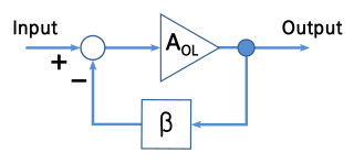
A negative-feedback amplifier is an electronic amplifier that subtracts a fraction of its output from its input, so that negative feedback opposes the original signal. The applied negative feedback can improve its performance and reduces sensitivity to parameter variations due to manufacturing or environment. Because of these advantages, many amplifiers and control systems use negative feedback.

<span class="mw-page-title-main">Impedance matching</span> Adjusting input/output impedances of an electrical circuit for some purpose

In electrical engineering, impedance matching is the practice of designing or adjusting the input impedance or output impedance of an electrical device for a desired value. Often, the desired value is selected to maximize power transfer or minimize signal reflection. For example, impedance matching typically is used to improve power transfer from a radio transmitter via the interconnecting transmission line to the antenna. Signals on a transmission line will be transmitted without reflections if the transmission line is terminated with a matching impedance.

<span class="mw-page-title-main">Voltage divider</span> Linear circuit that produces an output voltage that is a fraction of its input voltage

In electronics, a voltage divider (also known as a potential divider) is a passive linear circuit that produces an output voltage (Vout) that is a fraction of its input voltage (Vin). Voltage division is the result of distributing the input voltage among the components of the divider. A simple example of a voltage divider is two resistors connected in series, with the input voltage applied across the resistor pair and the output voltage emerging from the connection between them.

<span class="mw-page-title-main">Buffer amplifier</span> Electronic amplifier, a circuit component

A buffer amplifier is one that provides electrical impedance transformation from one circuit to another, with the aim of preventing the signal source from being affected by whatever currents that the load may impose. The signal is 'buffered from' load currents. Two main types of buffer exist: the voltage buffer and the current buffer.

<span class="mw-page-title-main">Common collector</span>

In electronics, a common collector amplifier is one of three basic single-stage bipolar junction transistor (BJT) amplifier topologies, typically used as a voltage buffer.

<span class="mw-page-title-main">Antenna tuner</span> Telecommunications device

An antenna tuner is an electronic device inserted into the feedline between a radio transmitter and its antenna. Its purpose is to optimize power transfer by matching the impedance of the radio to the signal impedance at the end of the feedline connecting the antenna to the transmitter.

In audio engineering and sound recording, a high impedance bridging, voltage bridging, or simply bridging connection is one in which the load impedance is much larger than the source impedance. The load measures the source's voltage while minimally drawing current or affecting it.

<span class="mw-page-title-main">Output impedance</span> Measure of the opposition to current flow by an internal electrical load

In electrical engineering, the output impedance of an electrical network is the measure of the opposition to current flow (impedance), both static (resistance) and dynamic (reactance), into the load network being connected that is internal to the electrical source. The output impedance is a measure of the source's propensity to drop in voltage when the load draws current, the source network being the portion of the network that transmits and the load network being the portion of the network that consumes.

In electrical engineering and electronics, a network is a collection of interconnected components. Network analysis is the process of finding the voltages across, and the currents through, all network components. There are many techniques for calculating these values; however, for the most part, the techniques assume linear components. Except where stated, the methods described in this article are applicable only to linear network analysis.

Line level is the specified strength of an audio signal used to transmit analog audio between components such as CD and DVD players, television sets, audio amplifiers, and mixing consoles.

Scattering parameters or S-parameters describe the electrical behavior of linear electrical networks when undergoing various steady state stimuli by electrical signals.

The cascode is a two-stage amplifier that consists of a common-emitter stage feeding into a common-base stage.

This article illustrates some typical operational amplifier applications. A non-ideal operational amplifier's equivalent circuit has a finite input impedance, a non-zero output impedance, and a finite gain. A real op-amp has a number of non-ideal features as shown in the diagram, but here a simplified schematic notation is used, many details such as device selection and power supply connections are not shown. Operational amplifiers are optimised for use with negative feedback, and this article discusses only negative-feedback applications. When positive feedback is required, a comparator is usually more appropriate. See Comparator applications for further information.

In electronics, the Miller effect accounts for the increase in the equivalent input capacitance of an inverting voltage amplifier due to amplification of the effect of capacitance between the input and output terminals. The virtually increased input capacitance due to the Miller effect is given by

An electrical load is an electrical component or portion of a circuit that consumes (active) electric power, such as electrical appliances and lights inside the home. The term may also refer to the power consumed by a circuit. This is opposed to a power supply source, such as a battery or generator, which provides power.

<span class="mw-page-title-main">Attenuator (electronics)</span> Type of electronic component

An attenuator is an electronic device that reduces the power of a signal without appreciably distorting its waveform.

A Wilson current mirror is a three-terminal circuit that accepts an input current at the input terminal and provides a "mirrored" current source or sink output at the output terminal. The mirrored current is a precise copy of the input current. It may be used as a Wilson current source by applying a constant bias current to the input branch as in Fig. 2. The circuit is named after George R. Wilson, an integrated circuit design engineer who worked for Tektronix. Wilson devised this configuration in 1967 when he and Barrie Gilbert challenged each other to find an improved current mirror overnight that would use only three transistors. Wilson won the challenge.

<span class="mw-page-title-main">L pad</span>

An L pad is a network composed of two impedances that typically resemble the letter capital "L" when drawn on a schematic circuit diagram. It is commonly used for attenuation and for impedance matching.

The Miller theorem refers to the process of creating equivalent circuits. It asserts that a floating impedance element, supplied by two voltage sources connected in series, may be split into two grounded elements with corresponding impedances. There is also a dual Miller theorem with regards to impedance supplied by two current sources connected in parallel. The two versions are based on the two Kirchhoff's circuit laws.

References