This article's lead sectionmay be too short to adequately summarize the key points. Please consider expanding the lead to provide an accessible overview of all important aspects of the article.(November 2025)
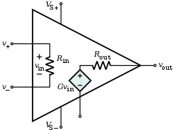
Fig.1: an equivalent circuit of an operational amplifier that models some non-ideal parameters using resistances. A real operational amplifier has a finite input impedance , a non-zero output impedance , and a finite gain .
In this article, a simplified schematic notation is used that ignores details such as device selection and power supply connections. Non-ideal properties (such as those shown in Fig.1) are ignored.
Operational amplifiers parameter requirements
In order for a particular device to be used in an application, it must satisfy certain requirements. The operational amplifier must
have large open-loop signal gain (voltage gain of 200,000 is obtained in early integrated circuit exemplars), and
have input impedance large with respect to values present in the feedback network.
With these requirements satisfied, one can use the method of virtual ground to quickly and intuitively grasp the behavior of the op-amp circuits.
Component specification
Resistors used in practical solid-state op-amp circuits are typically in the kΩ range. Resistors much greater than 1 MΩ cause excessive thermal noise and make the circuit operation susceptible to significant errors due to bias or leakage currents.
Input bias currents and input offset
Practical operational amplifiers draw a small current from each of their inputs due to bias requirements (in the case of bipolar junction transistor-based inputs) or leakage (in the case of MOSFET-based inputs).
These currents flow through the resistances connected to the inputs and produce small voltage drops across those resistances. Appropriate design of the feedback network can alleviate problems associated with input bias currents and common-mode gain, as explained below. The heuristic rule is to ensure that the impedance "looking out" of each input terminal is identical.
To the extent that the input bias currents do not match, there will be an effective input offset voltage present, which can lead to problems in circuit performance. Many commercial op-amp offerings provide a method for tuning the operational amplifier to balance the inputs (e.g., "offset null" or "balance" pins that can interact with an external voltage source attached to a potentiometer). Alternatively, a tunable external voltage can be added to one of the inputs in order to balance out the offset effect. In cases where a design calls for one input to be short-circuited to ground, that short circuit can be replaced with a variable resistance that can be tuned to mitigate the offset problem.
Operational amplifiers using MOSFET-based input stages have input leakage currents that will be, in many designs, negligible.
Power supply effects
Although power supplies are not indicated in the (simplified) operational amplifier designs below, they are nonetheless present and can be critical in operational amplifier circuit design.
Supply noise
Power supply imperfections (e.g., power signal ripple, non-zero source impedance) may lead to noticeable deviations from ideal operational amplifier behavior. For example, operational amplifiers have a specified power supply rejection ratio that indicates how well the output can reject signals that appear on the power supply inputs. Power supply inputs are often noisy in large designs because the power supply is used by nearly every component in the design, and inductance effects prevent current from being instantaneously delivered to every component at once. As a consequence, when a component requires large injections of current (e.g., a digital component that is frequently switching from one state to another), nearby components can experience sagging at their connection to the power supply. This problem can be mitigated with appropriate use of bypass capacitors connected across each power supply pin and ground. When bursts of current are required by a component, the component can bypass the power supply by receiving the current directly from the nearby capacitor (which is then slowly recharged by the power supply).
Using power supply currents in the signal path
Additionally, current drawn into the operational amplifier from the power supply can be used as inputs to external circuitry that augment the capabilities of the operational amplifier. For example, an operational amplifier may not be fit for a particular high-gain application because its output would be required to generate signals outside of the safe range generated by the amplifier. In this case, an external push–pull amplifier can be controlled by the current into and out of the operational amplifier. Thus, the operational amplifier may itself operate within its factory specified bounds while still allowing the negative feedback path to include a large output signal well outside of those bounds.[1]
The circuit shown computes the difference of two voltages, multiplied by some gain factor. The output voltage
Or, expressed as a function of the common-mode input Vcom and difference input Vdif:
the output voltage is
In order for this circuit to produce a signal proportional to the voltage difference of the input terminals, the coefficient of the Vcom term (the common-mode gain) must be zero, or
where the simple expression Rf / R1 represents the closed-loop gain of the differential amplifier.
The special case when the closed-loop gain is unity is a differential follower, with
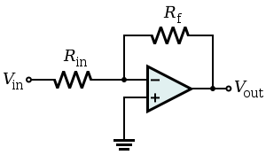
Inverting amplifier
An inverting amplifier is a special case of the differential amplifier in which that circuit's non-inverting input V2 is grounded, and inverting input V1 is identified with Vin above. The closed-loop gain is Rf / Rin, hence
.
The simplified circuit above is like the differential amplifier in the limit of R2 and Rg very small. In this case, though, the circuit will be susceptible to input bias current drift because of the mismatch between Rf and Rin.
To intuitively see the gain equation above, calculate the current in Rin:
then recall that this same current must be passing through Rf, therefore (because V− = V+ = 0):
A mechanical analogy is a seesaw, with the V− node (between Rin and Rf) as the fulcrum, at ground potential. Vin is at a length Rin from the fulcrum; Vout is at a length Rf. When Vin descends "below ground", the output Vout rises proportionately to balance the seesaw, and vice versa.[2]
As the negative input of the op-amp acts as a virtual ground, the input impedance of this circuit is equal to Rin.
Non-inverting amplifier
A non-inverting amplifier is a special case of the differential amplifier in which that circuit's inverting input V1 is grounded, and non-inverting input V2 is identified with Vin above, with R1 ≫ R2. Referring to the circuit immediately above,
.
To intuitively see this gain equation, use the virtual ground technique to calculate the current in resistor R1:
then recall that this same current must be passing through R2, therefore:
Unlike the inverting amplifier, a non-inverting amplifier cannot have a gain of less than 1.
A mechanical analogy is a class-2 lever, with one terminal of R1 as the fulcrum, at ground potential. Vin is at a length R1 from the fulcrum; Vout is at a length R2 further along. When Vin ascends "above ground", the output Vout rises proportionately with the lever.
The input impedance of the simplified non-inverting amplifier is high:
where Zdif is the op-amp's input impedance to differential signals, and AOL is the open-loop voltage gain of the op-amp (which varies with frequency), and B is the feedback factor (the fraction of the output signal that returns to the input).[3][4] In the case of the ideal op-amp, with AOL infinite and Zdif infinite, the input impedance is also infinite. In this case, though, the circuit will be susceptible to input bias current drift because of the mismatch between the impedances driving the V+ and V− op-amp inputs.
The feedback loop similarly decreases the output impedance:
where Zout is the output impedance with feedback, and ZOL is the open-loop output impedance.[4]
(realistically, the differential input impedance of the op-amp itself (1 MΩ to 1 TΩ), multiplied by the open-loop gain of the op-amp)
Due to the strong (i.e., unity gain) feedback and certain non-ideal characteristics of real operational amplifiers, this feedback system is prone to have poor stability margins. Consequently, the system may be unstable when connected to sufficiently capacitive loads. In these cases, a lag compensation network (e.g., connecting the load to the voltage follower through a resistor) can be used to restore stability. The manufacturer data sheet for the operational amplifier may provide guidance for the selection of components in external compensation networks. Alternatively, another operational amplifier can be chosen that has more appropriate internal compensation.
The input and output impedance are affected by the feedback loop in the same way as the non-inverting amplifier, with B=1.[3][4]
Summing amplifier
A summing amplifier produces the negative of the sum of several (weighted) voltages:
When , and independent
When
Input impedance of the nth input is ( is a virtual ground)
Operational amplifiers can be used in construction of active filters, providing high-pass, low-pass, band-pass, reject and delay functions. The high input impedance and gain of an op-amp allow straightforward calculation of element values, allowing accurate implementation of any desired filter topology with little concern for the loading effects of stages in the filter or of subsequent stages. However, the frequencies at which active filters can be implemented is limited; when the behavior of the amplifiers departs significantly from the ideal behavior assumed in elementary design of the filters, filter performance is degraded.
An operational amplifier can, if necessary, be forced to act as a comparator. The smallest difference between the input voltages will be amplified enormously, causing the output to swing to nearly the supply voltage. However, it is usually better to use a dedicated comparator for this purpose, as its output has a higher slew rate and can reach either power supply rail. Some op-amps have clamping diodes on the input that prevent use as a comparator.[5]
Assuming ideal elements, it integrates the input signal (multiplied by ) over a time interval from t0 to t1, yielding an output voltage at time t = t1 of:
where Vout(t0) is the capacitor's initial voltage at time t = t0. In other words, the circuit's output voltage changes over the time interval by an amount proportional to the time integral of the input voltage:
Its practicality is limited by a significant problem: unless the capacitor is periodically discharged, the output voltage will eventually drift outside of the operational amplifier's operating range. This can be due to any combination of:
The following slightly more complex circuit can ameliorate the second two problems, and in some cases, the first as well, but has a limited bandwidth of integration:
Here, the feedback resistor Rf provides a discharge path for capacitor Cf. The series resistor Rn at the non-inverting input alleviates input bias current and common-mode problems, provided it is set to the parallel resistance of Ri|| Rf:
Because the circuit is a first-order low-pass filter with a flat response up to its cutoff frequency , it only functions as an integrator for frequencies significantly higher than that cutoff.
Assuming ideal elements, this circuit differentiates the signal (multiplied by ) over time:
where and are functions of time.
The transfer function of the inverting differentiator has a single zero in the origin (i.e., where angular frequency). The high-pass characteristics of a differentiating amplifier can lead to stability challenges when the circuit is used in an analog servo loop (e.g., in a PID controller with a significant derivative gain). In particular, as a root locus analysis would show, increasing feedback gain will drive a closed-loop pole toward marginal stability at the DC zero introduced by the differentiator.
Simulates an inductor (i.e., provides inductance without the use of a possibly costly inductor). The circuit exploits the fact that the current flowing through a capacitor behaves through time as the voltage across an inductor. The capacitor used in this circuit is geometrically smaller than the inductor it simulates, and its capacitance is less subject to changes in value due to environmental changes. Applications where this circuit may be superior to a physical inductor are simulating a variable inductance or simulating a very large inductance.
This circuit is of limited use in applications relying on the back EMF property of an inductor, as this effect will be limited in a gyrator circuit to the voltage supplies of the op-amp.
The voltage drop VF across the forward-biased diode in the circuit of a passive rectifier is undesired. In this active version, the problem is solved by connecting the diode in the negative feedback loop. The op-amp compares the output voltage across the load with the input voltage and increases its own output voltage with the value of VF. As a result, the voltage drop VF is compensated, and the circuit behaves very nearly as an ideal (super) diode with VF = 0V.
The circuit has speed limitations at high frequency because of the slow negative feedback and due to the low slew rate of many non-ideal op-amps.
where is the saturation current, is the forward voltage across the diode, and is the thermal voltage (approximately 26mV at room temperature). When the diode's current is approximately proportional to an exponential function:
The opamp's inverting input is virtually grounded and ideally draws no current. Thus, the output voltage will be:
The output voltage is thus approximately an exponential function of the input voltage :
This implementation does not consider temperature stability and other non-ideal effects.
Since the logarithm is the inverse function of exponentiation, the exponential output circuit described above can be rearranged by swapping the diode into the feedback path of the opamp to form a log amplifier:
Since the opamp's inverting input is virtually grounded and ideally draws no current, and the current flowing from the source through the resistor and diode is:
where is the current through the diode, which as described earlier is approximately:
Solving for gives an approximately logarithmic relationship between the input voltage and the output voltage :
This implementation does not consider temperature stability and other non-ideal effects.
Temperature-compensated three-segment compression function
The schematic shown for a "temperature-compensated three-segment compression function"[8][9] produces a gain compression transfer function where each subsequent line segment reduces the steepness of the transfer function. For small signals, transistors Q2 and Q3 produce very little base current, and so the circuit's gain is determined just by the feedback resistance of R2 divided by the input resistance of R1. Once the output voltage exceeds around 2V (whose exact voltage depends on R3 and R4 and the -15V supply), then Q3 saturates, so the circuit's feedback resistance is determined by R4 in parallel with R2, reducing the gain. As the output voltage increases more, Q2 will saturate, so the circuit's gain is again reduced by the additional inclusion of R6 into the parallel feedback resistance. Temperature-compensation transistors Q4 and Q1 cancel out the temperature-dependent p–n junction base-emitter forward voltage drop of Q3 and Q2. Additional linear segments can be added using additional copies of the resistor-transistor-resistor chains (like the chain R5, Q2, R6 or the chain R3, Q3, R4 but with different values) in a similar manner to further compress the input. This circuit's compression function only works for negative inputs. Diode D1 forces the output to zero if a positive input is applied.
↑ If you think of the left-hand side of the relation as the closed-loop gain of the inverting input, and the right-hand side as the gain of the non-inverting input, then matching these two quantities provides an output insensitive to the common-mode voltage of and .
1 2 3 Simpson, Robert E. (1987). "7.2 Negative Voltage Feedback". Introductory electronics for scientists and engineers (2nded.). Boston: Allyn and Bacon. p.291. ISBN0205083773. OCLC13821010. input impedance of an amplifier without negative feedback is increased by adding negative feedback. .. .. output impedance .. is decreased ..
This page is based on this Wikipedia article Text is available under the CC BY-SA 4.0 license; additional terms may apply. Images, videos and audio are available under their respective licenses.