An integrated circuit or monolithic integrated circuit is a set of electronic circuits on one small flat piece of semiconductor material that is normally silicon. The integration of large numbers of tiny transistors into a small chip results in circuits that are orders of magnitude smaller, cheaper, and faster than those constructed of discrete electronic components. The IC's mass production capability, reliability and building-block approach to circuit design has ensured the rapid adoption of standardized ICs in place of designs using discrete transistors. ICs are now used in virtually all electronic equipment and have revolutionized the world of electronics. Computers, mobile phones, and other digital home appliances are now inextricable parts of the structure of modern societies, made possible by the small size and low cost of ICs.

Semiconductor device fabrication is the process used to create the integrated circuits that are present in everyday electrical and electronic devices. It is a multiple-step sequence of photolithographic and chemical processing steps during which electronic circuits are gradually created on a wafer made of pure semiconducting material. Silicon is almost always used, but various compound semiconductors are used for specialized applications.
A semiconductor material has an electrical conductivity value falling between that of a metal, like copper, gold, etc. and an insulator, such as glass. Their resistance decreases as their temperature increases, which is behaviour opposite to that of a metal. Their conducting properties may be altered in useful ways by the deliberate, controlled introduction of impurities ("doping") into the crystal structure. Where two differently-doped regions exist in the same crystal, a semiconductor junction is created. The behavior of charge carriers which include electrons, ions and electron holes at these junctions is the basis of diodes, transistors and all modern electronics. Some examples of semiconductors are silicon, germanium, and gallium arsenide. After silicon, gallium arsenide is the second most common semiconductor used in laser diodes, solar cells, microwave frequency integrated circuits, and others. Silicon is a critical element for fabricating most electronic circuits.

The carbon group is a periodic table group consisting of carbon (C), silicon (Si), germanium (Ge), tin (Sn), lead (Pb), and flerovium (Fl).

Gallium arsenide (GaAs) is a compound of the elements gallium and arsenic. It is a III-V direct bandgap semiconductor with a zinc blende crystal structure.
SiGe, or silicon-germanium, is an alloy with any molar ratio of silicon and germanium, i.e. with a molecular formula of the form Si1−xGex. It is commonly used as a semiconductor material in integrated circuits (ICs) for heterojunction bipolar transistors or as a strain-inducing layer for CMOS transistors. IBM introduced the technology into mainstream manufacturing in 1989. This relatively new technology offers opportunities in mixed-signal circuit and analog circuit IC design and manufacture. SiGe is also used as a thermoelectric material for high temperature applications.
Silicon on insulator (SOI) technology refers to the use of a layered silicon–insulator–silicon substrate in place of conventional silicon substrates in semiconductor manufacturing, especially microelectronics, to reduce parasitic device capacitance, thereby improving performance. SOI-based devices differ from conventional silicon-built devices in that the silicon junction is above an electrical insulator, typically silicon dioxide or sapphire. The choice of insulator depends largely on intended application, with sapphire being used for high-performance radio frequency (RF) and radiation-sensitive applications, and silicon dioxide for diminished short channel effects in microelectronics devices. The insulating layer and topmost silicon layer also vary widely with application.
This article is about ionizing radiation detectors. For information about semiconductor detectors in radio, see Detector (radio), Crystal detector, Diode#Semiconductor diodes, and Rectifier.
The heterojunction bipolar transistor (HBT) is a type of bipolar junction transistor (BJT) which uses differing semiconductor materials for the emitter and base regions, creating a heterojunction. The HBT improves on the BJT in that it can handle signals of very high frequencies, up to several hundred GHz. It is commonly used in modern ultrafast circuits, mostly radio-frequency (RF) systems, and in applications requiring a high power efficiency, such as RF power amplifiers in cellular phones. The idea of employing a heterojunction is as old as the conventional BJT, dating back to a patent from 1951. Detailed theory of heterojunction bipolar transistor was developed by Herbert Kroemer in 1957.
The term high-κ dielectric refers to a material with a high dielectric constant κ. High-κ dielectrics are used in semiconductor manufacturing processes where they are usually used to replace a silicon dioxide gate dielectric or another dielectric layer of a device. The implementation of high-κ gate dielectrics is one of several strategies developed to allow further miniaturization of microelectronic components, colloquially referred to as extending Moore's Law.

Strained silicon is a layer of silicon in which the silicon atoms are stretched beyond their normal interatomic distance. This can be accomplished by putting the layer of silicon over a substrate of silicon germanium (SiGe). As the atoms in the silicon layer align with the atoms of the underlying silicon germanium layer, the links between the silicon atoms become stretched - thereby leading to strained silicon. Moving these silicon atoms farther apart reduces the atomic forces that interfere with the movement of electrons through the transistors and thus better mobility, resulting in better chip performance and lower energy consumption. These electrons can move 70% faster allowing strained silicon transistors to switch 35% faster.
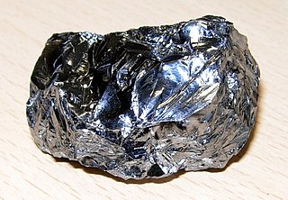
Germanium tetrachloride is a colourless, fuming liquid with a peculiar, acidic odour. It is used as an intermediate in the production of purified germanium metal. In recent years, GeCl4 usage has increased substantially due to its use as a reagent for fiber optic production.

Silicon photonics is the study and application of photonic systems which use silicon as an optical medium. The silicon is usually patterned with sub-micrometre precision, into microphotonic components. These operate in the infrared, most commonly at the 1.55 micrometre wavelength used by most fiber optic telecommunication systems. The silicon typically lies on top of a layer of silica in what is known as silicon on insulator (SOI).
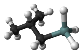
Isobutylgermane (IBGe, Chemical formula: (CH3)2CHCH2GeH3), is an organogermanium compound. It is a colourless, volatile liquid that is used in MOVPE (Metalorganic Vapor Phase Epitaxy) as an alternative to germane. IBGe is used in the deposition of Ge films and Ge-containing thin semiconductor films such as SiGe in strained silicon application, and GeSbTe in NAND Flash applications.
Strain engineering refers to a general strategy employed in semiconductor manufacturing to enhance device performance. Performance benefits are achieved by modulating strain in the transistor channel, which enhances electron mobility and thereby conductivity through the channel.
A substrate is a solid substance onto which a layer of another substance is applied, and to which that second substance adheres. In solid-state electronics, this term refers to a thin slice of material such as silicon, silicon dioxide, aluminum oxide, sapphire, germanium, gallium arsenide (GaAs), an alloy of silicon and germanium, or indium phosphide (InP). These serve as the foundation upon which electronic devices such as transistors, diodes, and especially integrated circuits (ICs) are deposited.

Digermane is an inorganic compound with the chemical formula Ge2H6. One of the few hydrides of germanium, it is a colourless liquid. Its molecular geometry is similar to ethane.

John D. Cressler is a Georgia Tech professor and author.