
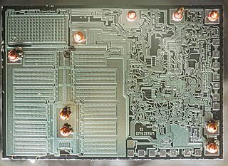
An integrated circuit (IC), also known as a microchip or simply chip, is a small electronic device made up of multiple interconnected electronic components such as transistors, resistors, and capacitors. These components are etched onto a small piece of semiconductor material, usually silicon. Integrated circuits are used in a wide range of electronic devices, including computers, smartphones, and televisions, to perform various functions such as processing and storing information. They have greatly impacted the field of electronics by enabling device miniaturization and enhanced functionality.

Semiconductor device fabrication is the process used to manufacture semiconductor devices, typically integrated circuits (ICs) such as microprocessors, microcontrollers, and memories. It is a multiple-step photolithographic and physico-chemical process during which electronic circuits are gradually created on a wafer, typically made of pure single-crystal semiconducting material. Silicon is almost always used, but various compound semiconductors are used for specialized applications.

An application-specific integrated circuit is an integrated circuit (IC) chip customized for a particular use, rather than intended for general-purpose use, such as a chip designed to run in a digital voice recorder or a high-efficiency video codec. Application-specific standard product chips are intermediate between ASICs and industry standard integrated circuits like the 7400 series or the 4000 series. ASIC chips are typically fabricated using metal–oxide–semiconductor (MOS) technology, as MOS integrated circuit chips.

Flip chip, also known as controlled collapse chip connection or its abbreviation, C4, is a method for interconnecting dies such as semiconductor devices, IC chips, integrated passive devices and microelectromechanical systems (MEMS), to external circuitry with solder bumps that have been deposited onto the chip pads. The technique was developed by General Electric's Light Military Electronics Department, Utica, New York. The solder bumps are deposited on the chip pads on the top side of the wafer during the final wafer processing step. In order to mount the chip to external circuitry, it is flipped over so that its top side faces down, and aligned so that its pads align with matching pads on the external circuit, and then the solder is reflowed to complete the interconnect. This is in contrast to wire bonding, in which the chip is mounted upright and fine wires are welded onto the chip pads and lead frame contacts to interconnect the chip pads to external circuitry.

Die preparation is a step of semiconductor device fabrication during which a wafer is prepared for IC packaging and IC testing. The process of die preparation typically consists of two steps: wafer mounting and wafer dicing.

Automatic test equipment or automated test equipment (ATE) is any apparatus that performs tests on a device, known as the device under test (DUT), equipment under test (EUT) or unit under test (UUT), using automation to quickly perform measurements and evaluate the test results. An ATE can be a simple computer-controlled digital multimeter, or a complicated system containing dozens of complex test instruments capable of automatically testing and diagnosing faults in sophisticated electronic packaged parts or on wafer testing, including system on chips and integrated circuits.
Wafer-scale integration (WSI) is a system of building very-large integrated circuit networks from an entire silicon wafer to produce a single "super-chip". Combining large size and reduced packaging, WSI was expected to lead to dramatically reduced costs for some systems, notably massively parallel supercomputers but is now being employed for deep learning. The name is taken from the term very-large-scale integration, the state of the art when WSI was being developed.

Back end of the line or back end of line (BEOL) is a process in semiconductor device fabrication that consists of depositing metal interconnect layers onto a wafer already patterned with devices. It is the second part of IC fabrication, after front end of line (FEOL). In BEOL, the individual devices are connected to each other according to how the metal wiring is deposited.

Integrated circuit design, semiconductor design, chip design or IC design, is a sub-field of electronics engineering, encompassing the particular logic and circuit design techniques required to design integrated circuits, or ICs. ICs consist of miniaturized electronic components built into an electrical network on a monolithic semiconductor substrate by photolithography.

A system in a package (SiP) or system-in-package is a number of integrated circuits (ICs) enclosed in one chip carrier package or encompassing an IC package substrate that may include passive components and perform the functions of an entire system. The ICs may be stacked using package on package, placed side by side, and/or embedded in the substrate. The SiP performs all or most of the functions of an electronic system, and is typically used when designing components for mobile phones, digital music players, etc. Dies containing integrated circuits may be stacked vertically on the package substrate. They are internally connected by fine wires that are bonded to the package substrate. Alternatively, with a flip chip technology, solder bumps are used to join stacked chips together and to the package substrate, or even both techniques can be used in a single package. SiPs are like systems on a chip (SoCs) but less tightly integrated and not on a single semiconductor die.
A device under test (DUT), also known as equipment under test (EUT) and unit under test (UUT), is a manufactured product undergoing testing, either at first manufacture or later during its life cycle as part of ongoing functional testing and calibration checks. This can include a test after repair to establish that the product is performing in accordance with the original product specification.

A probe card is used in automated integrated circuit testing. It is an interface between an electronic test system and a semiconductor wafer.
A die, in the context of integrated circuits, is a small block of semiconducting material on which a given functional circuit is fabricated. Typically, integrated circuits are produced in large batches on a single wafer of electronic-grade silicon (EGS) or other semiconductor through processes such as photolithography. The wafer is cut (diced) into many pieces, each containing one copy of the circuit. Each of these pieces is called a die.

Multi-project chip (MPC), and multi-project wafer (MPW) semiconductor manufacturing arrangements allow customers to share tooling and microelectronics wafer fabrication cost between several designs or projects.

In electronic engineering, a through-silicon via (TSV) or through-chip via is a vertical electrical connection (via) that passes completely through a silicon wafer or die. TSVs are high-performance interconnect techniques used as an alternative to wire-bond and flip chips to create 3D packages and 3D integrated circuits. Compared to alternatives such as package-on-package, the interconnect and device density is substantially higher, and the length of the connections becomes shorter.
A three-dimensional integrated circuit is a MOS integrated circuit (IC) manufactured by stacking as many as 16 or more ICs and interconnecting them vertically using, for instance, through-silicon vias (TSVs) or Cu-Cu connections, so that they behave as a single device to achieve performance improvements at reduced power and smaller footprint than conventional two dimensional processes. The 3D IC is one of several 3D integration schemes that exploit the z-direction to achieve electrical performance benefits in microelectronics and nanoelectronics.
Non contact wafer testing is an alternative to mechanical probing of ICs during the wafer testing step in semiconductor device fabrication.
A semiconductor package is a metal, plastic, glass, or ceramic casing containing one or more discrete semiconductor devices or integrated circuits. Individual components are fabricated on semiconductor wafers before being diced into die, tested, and packaged. The package provides a means for connecting it to the external environment, such as printed circuit board, via leads such as lands, balls, or pins; and protection against threats such as mechanical impact, chemical contamination, and light exposure. Additionally, it helps dissipate heat produced by the device, with or without the aid of a heat spreader. There are thousands of package types in use. Some are defined by international, national, or industry standards, while others are particular to an individual manufacturer.

Tokyo Electron Limited, or TEL, is a Japanese electronics and semiconductor company headquartered in Akasaka, Minato-ku, Tokyo, Japan. The company was founded as Tokyo Electron Laboratories, Inc. in 1963. TEL is best known as a supplier of equipment to fabricate integrated circuits (IC), flat panel displays (FPD), and photovoltaic cells (PV). Tokyo Electron Device, or TED, is a subsidiary of TEL specializing in semiconductor devices, electronic components, and networking devices. As of 2011, TEL was the largest manufacturer of IC and FPD production equipment. Listed on the Nikkei 225, in 2024, Tokyo Electron had a market cap of US$114.6 billion, making it the third-most valuable company in Japan in terms of market cap, and the 12th ranked semiconductor-related company worldwide.
Glossary of microelectronics manufacturing terms
