
An integrated circuit or monolithic integrated circuit is a set of electronic circuits on one small flat piece of semiconductor material that is normally silicon. Large numbers of tiny MOSFETs integrate into a small chip. This results in circuits that are orders of magnitude smaller, faster, and less expensive than those constructed of discrete electronic components. The IC's mass production capability, reliability, and building-block approach to integrated circuit design has ensured the rapid adoption of standardized ICs in place of designs using discrete transistors. ICs are now used in virtually all electronic equipment and have revolutionized the world of electronics. Computers, mobile phones, and other digital home appliances are now inextricable parts of the structure of modern societies, made possible by the small size and low cost of ICs.

Microelectromechanical systems (MEMS), also written as micro-electro-mechanical systems and the related micromechatronics and microsystems constitute the technology of microscopic devices, particularly those with moving parts. They merge at the nanoscale into nanoelectromechanical systems (NEMS) and nanotechnology. MEMS are also referred to as micromachines in Japan and microsystem technology (MST) in Europe.

Semiconductor device fabrication is the process used to manufacture semiconductor devices, typically the metal–oxide–semiconductor (MOS) devices used in the integrated circuit (IC) chips that are present in everyday electrical and electronic devices. It is a multiple-step sequence of photolithographic and chemical processing steps during which electronic circuits are gradually created on a wafer made of pure semiconducting material. Silicon is almost always used, but various compound semiconductors are used for specialized applications.
A semiconductor material has an electrical conductivity value falling between that of a conductor, such as metallic copper, and an insulator, such as glass. Its resistivity falls as its temperature rises; metals behave in the opposite way. Its conducting properties may be altered in useful ways by introducing impurities ("doping") into the crystal structure. When two differently-doped regions exist in the same crystal, a semiconductor junction is created. The behavior of charge carriers, which include electrons, ions and electron holes, at these junctions is the basis of diodes, transistors and most modern electronics. Some examples of semiconductors are silicon, germanium, gallium arsenide, and elements near the so-called "metalloid staircase" on the periodic table. After silicon, gallium arsenide is the second most common semiconductor and is used in laser diodes, solar cells, microwave-frequency integrated circuits, and others. Silicon is a critical element for fabricating most electronic circuits.
A semiconductor device is an electronic component that relies on the electronic properties of a semiconductor material for its function. Semiconductor devices have replaced vacuum tubes in most applications. They use electrical conduction in the solid state rather than the gaseous state or thermionic emission in a vacuum.

In electronics, a wafer is a thin slice of semiconductor, such as a crystalline silicon (c-Si), used for the fabrication of integrated circuits and, in photovoltaics, to manufacture solar cells. The wafer serves as the substrate for microelectronic devices built in and upon the wafer. It undergoes many microfabrication processes, such as doping, ion implantation, etching, thin-film deposition of various materials, and photolithographic patterning. Finally, the individual microcircuits are separated by wafer dicing and packaged as an integrated circuit.

A thin-film transistor (TFT) is a special type of metal–oxide–semiconductor field-effect transistor (MOSFET) made by depositing thin films of an active semiconductor layer as well as the dielectric layer and metallic contacts over a supporting substrate. A common substrate is glass, because the primary application of TFTs is in liquid-crystal displays (LCDs). This differs from the conventional bulk MOSFET transistor, where the semiconductor material typically is the substrate, such as a silicon wafer.
In semiconductor technology, copper interconnects are interconnects made of copper. They are used in silicon integrated circuits (ICs) to reduce propagation delays and power consumption. Since copper is a better conductor than aluminium, ICs using copper for their interconnects can have interconnects with narrower dimensions, and use less energy to pass electricity through them. Together, these effects lead to ICs with better performance. They were first introduced by IBM, with assistance from Motorola, in 1997.
In semiconductor manufacturing, silicon on insulator (SOI) technology is fabrication of silicon semiconductor devices in a layered silicon–insulator–silicon substrate, to reduce parasitic capacitance within the device, thereby improving performance. SOI-based devices differ from conventional silicon-built devices in that the silicon junction is above an electrical insulator, typically silicon dioxide or sapphire. The choice of insulator depends largely on intended application, with sapphire being used for high-performance radio frequency (RF) and radiation-sensitive applications, and silicon dioxide for diminished short-channel effects in other microelectronics devices. The insulating layer and topmost silicon layer also vary widely with application.
Chemical mechanical polishing (CMP) or planarization is a process of smoothing surfaces with the combination of chemical and mechanical forces. It can be thought of as a hybrid of chemical etching and free abrasive polishing.

Microfabrication is a technique that use semiconductor manufacturing processes such as ion etching, diffusion, oxidation, sputtering etc. in combination with specialized micromachining techniques. This machining occurs in the range of 1-100 micrometers in size, where both the mechanical parts and the electronics that control them are built in the same piece of silicon. MEMS Fabrication consists in the application of the following steps, normally several times during the manufacturing. The process starts with a polished silicon – the substrate wafer that undergoes these steps such as Thin film growth or Deposition, Doping, Lithography and etching and Micromachining.
Soitec is a France-based international industrial company specialized in generating and manufacturing high performance semiconductor materials.
A hybrid silicon laser is a semiconductor laser fabricated from both silicon and group III-V semiconductor materials. The hybrid silicon laser was developed to address the lack of a silicon laser to enable fabrication of low-cost, mass-producible silicon optical devices. The hybrid approach takes advantage of the light-emitting properties of III-V semiconductor materials combined with the process maturity of silicon to fabricate electrically driven lasers on a silicon wafer that can be integrated with other silicon photonic devices.
In electronics, a self-aligned gate is a transistor manufacturing feature whereby a refractory gate electrode region of a MOSFET is used as a mask for the doping of the source and drain regions. This technique ensures that the gate will slightly overlap the edges of the source and drain.
Ghavam G. Shahidi is an Iranian-American electrical engineer and IBM Fellow. He is the director of Silicon Technology at the IBM Thomas J Watson Research Center. He is best known for his pioneering work in silicon-on-insulator (SOI) complementary metal–oxide–semiconductor (CMOS) technology since the late 1980s.
A three-dimensional integrated circuit is a MOS integrated circuit (IC) manufactured by stacking silicon wafers or dies and interconnecting them vertically using, for instance, through-silicon vias (TSVs) or Cu-Cu connections, so that they behave as a single device to achieve performance improvements at reduced power and smaller footprint than conventional two dimensional processes. The 3D IC is one of several 3D integration schemes that exploit the z-direction to achieve electrical performance benefits in microelectronics and nanoelectronics.
Monocrystalline silicon, more often called single-crystal silicon, in short mono c-Si or mono-Si, is the base material for silicon-based discrete components and integrated circuits used in virtually all modern electronic equipment. Mono-Si also serves as a photovoltaic, light-absorbing material in the manufacture of solar cells.
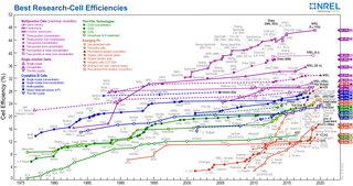
There are currently many research groups active in the field of photovoltaics in universities and research institutions around the world. This research can be categorized into three areas: making current technology solar cells cheaper and/or more efficient to effectively compete with other energy sources; developing new technologies based on new solar cell architectural designs; and developing new materials to serve as more efficient energy converters from light energy into electric current or light absorbers and charge carriers.
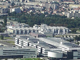
CEA-Leti is a research institute for electronics and information technologies, based in Grenoble, France. It is one of the world's largest organizations for applied research in microelectronics and nanotechnology.
Glossary of Microelectronics Manufacturing Terms
