Millipede memory

Last updated

Millipede memory is a form of non-volatile computer memory. It promised a data density of more than 1 terabit per square inch (1 gigabit per square millimeter), which is about the limit of the perpendicular recording hard drives. Millipede storage technology was pursued as a potential replacement for magnetic recording in hard drives and a means of reducing the physical size of the technology to that of flash media.

Contents

IBM demonstrated a prototype millipede storage device at CeBIT 2005, and was trying to make the technology commercially available by the end of 2007. However, because of concurrent advances in competing storage technologies, no commercial product has been made available since then.

Technology

Basic concept

The main memory of modern computers is constructed from one of a number of DRAM-related devices. DRAM basically consists of a series of capacitors, which store data in terms of the presence or absence of electrical charge. Each capacitor and its associated control circuitry, referred to as a cell, holds one bit, and multiple bits can be read or written in large blocks at the same time. DRAM is volatile — data is lost when power is removed.

In contrast, hard drives store data on a disk that is covered with a magnetic material; data is represented by this material being locally magnetized. Reading and writing are accomplished by a single head, which waits for the requested memory location to pass under the head while the disk spins. As a result, a hard drive's performance is limited by the mechanical speed of the motor, and it is generally hundreds of thousands of times slower than DRAM. However, since the "cells" in a hard drive are much smaller, the storage density for hard drives is much higher than DRAM. Hard drives are non-volatile — data is retained even after power is removed.

Millipede storage attempts to combine features of both. Like a hard drive, millipede both stores data in a medium and accesses the data by moving the medium under the head. Also similar to hard drives, millipede's physical medium stores a bit in a small area, leading to high storage densities. However, millipede uses many nanoscopic heads that can read and write in parallel, thereby increasing the amount of data read at a given time.

Mechanically, millipede uses numerous atomic force probes, each of which is responsible for reading and writing a large number of bits associated with it. These bits are stored as a pit, or the absence of one, in the surface of a thermo-active polymer, which is deposited as a thin film on a carrier known as the sled. Any one probe can only read or write a fairly small area of the sled available to it, known as a storage field. Normally the sled is moved so that the selected bits are positioned under the probe using electromechanical actuators. These actuators are similar to those that position the read/write head in a typical hard drive, however, the actual distance moved is tiny in comparison. The sled is moved in a scanning pattern to bring the requested bits under the probe, a process known as x/y scan.

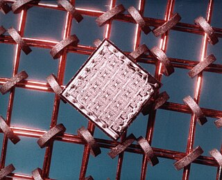
The amount of memory serviced by any one field/probe pair is fairly small, but so is its physical size. Thus, many such field/probe pairs are used to make up a memory device, and data reads and writes can be spread across many fields in parallel, increasing the throughput and improving the access times. For instance, a single 32-bit value would normally be written as a set of single bits sent to 32 different fields. In the initial experimental devices, the probes were mounted in a 32x32 grid for a total of 1,024 probes. Given this layout looked like the legs on a millipede (animal), the name stuck. The design of the cantilever array involves making numerous mechanical cantilevers, on which a probe has to be mounted. All the cantilevers are made entirely out of silicon, using surface micromachining at the wafer surface.

Regarding the creation of indentations, or pits, non-crosslinked polymers retain a low glass temperature, around 120 °C for PMMA [1] and if the probe tip is heated to above the glass temperature, it leaves a small indentation. Indentations are made at 3 nm lateral resolution. [2] By heating the probe immediately next to an indentation, the polymer will re-melt and fill in the indentation, erasing it (see also: thermo-mechanical scanning probe lithography). After writing, the probe tip can be used to read the indentations. If each indentation is treated as one bit then a storage density of 0.9 Tb/in2 could theoretically be achieved. [2]

Thermal writing and erasing of a bit Write erase bit.tiff
Thermal writing and erasing of a bit

Reading and writing data

Each probe in the cantilever array stores and reads data thermo-mechanically, handling one bit at a time. To accomplish a read, the probe tip is heated to around 300 °C and moved in proximity to the data sled. If the probe is located over a pit the cantilever will push it into the hole, increasing the surface area in contact with the sled, and in turn increasing the cooling as heat leaks into the sled from the probe. In the case where there is no pit at that location, only the very tip of the probe remains in contact with the sled, and the heat leaks away more slowly. The electrical resistance of the probe is a function of its temperature, and it rises with an increase in temperature. Thus when the probe drops into a pit and cools, this registers as a drop in resistance. A low resistance will be translated to a "1" bit, or a "0" bit otherwise. While reading an entire storage field, the tip is dragged over the entire surface and the resistance changes are constantly monitored.

To write a bit, the tip of the probe is heated to a temperature above the glass transition temperature of the polymer used to manufacture the data sled, which is generally made of acrylic glass. In this case the transition temperature is around 400 °C. To write a "1", the polymer in proximity to the tip is softened, and then the tip is gently touched to it, causing a dent. To erase the bit and return it to the zero state, the tip is instead pulled up from the surface, allowing surface tension to pull the surface flat again. Older experimental systems used a variety of erasure techniques that were generally more time consuming and less successful. These older systems offered around 100,000 erases, but the available references do not contain enough information to say if this has been improved with the newer techniques.[ citation needed ]

As one might expect, the need to heat the probes requires a fairly large amount of power for general operation. However, the exact amount is dependent on the speed that data is being accessed; at slower rates the cooling during read is smaller, as is the number of times the probe has to be heated to a higher temperature to write. When operated at data rates of a few megabits per second, Millipede is expected to consume about 100 milliwatts, which is in the range of flash memory technology and considerably below hard drives. However, one of the main advantages of the Millipede design is that it is highly parallel, allowing it to run at much higher speeds into the GB/s. At these sorts of speeds one might expect power requirements more closely matching current hard drives, and indeed, data transfer speed is limited to the kilobits-per-second range for an individual probe, which amounts to a few megabits for an entire array. Experiments done at IBM's Almaden Research Center showed that individual tips could support data rates as high as 1 - 2 megabits per second, potentially offering aggregate speeds in the GB/s range.

Applications

Millipede memory was proposed as a form of non-volatile computer memory that was intended to compete with flash memory in terms of data storage, reading and writing speed, and physical size of the technology. However, other technologies have since surpassed it, and thus it does not appear to be a technology currently being pursued.

History

First devices

The earliest generation millipede devices used probes 10 nanometers in diameter and 70 nanometers in length, producing pits about 40 nm in diameter on fields 92 µm x 92 µm. Arranged in a 32 x 32 grid, the resulting 3 mm x 3 mm chip stores 500 megabits of data or 62.5 MB, resulting in an areal density, the number of bits per square inch, on the order of 200 Gbit/in². IBM initially demonstrated this device in 2003, planning to introduce it commercially in 2005. By that point hard drives were approaching 150 Gbit/in², and have since surpassed it.

Proposed commercial product

Devices demonstrated at the CeBIT Expo in 2005 improved on the basic design, using a 64 x 64 cantilever chips with a 7 mm x 7 mm data sled, boosting the data storage capacity to 800 Gbit/in² using smaller pits. It appears the pit size can scale to about 10 nm, resulting in a theoretical areal density just over 1Tbit/in². IBM planned to introduce devices based on this sort of density in 2007. For comparison, as of late 2011, laptop hard drives were shipping with a density of 636 Gbit/in², [3] and it is expected that heat-assisted magnetic recording and patterned media together could support densities of 10 Tbit/in². [4] Flash reached almost 250 Gbit/in² in early 2010. [5]

Current development

As of 2015,[ citation needed ] because of concurrent advances in competing storage technologies, no commercial product has been made available so far.

See also

Related Research Articles

<span class="mw-page-title-main">Computer data storage</span> Storage of digital data readable by computers

Computer data storage is a technology consisting of computer components and recording media that are used to retain digital data. It is a core function and fundamental component of computers.

<span class="mw-page-title-main">Computer memory</span> Component of a computer storing information for immediate use.

Computer memory stores information, such as data and programs for immediate use in the computer. The term memory is often synonymous with the term primary storage or main memory. An archaic synonym for memory is store.

<span class="mw-page-title-main">Hard disk drive</span> Electro-mechanical data storage device

A hard disk drive (HDD), hard disk, hard drive, or fixed disk, is an electro-mechanical data storage device that stores and retrieves digital data using magnetic storage with one or more rigid rapidly rotating platters coated with magnetic material. The platters are paired with magnetic heads, usually arranged on a moving actuator arm, which read and write data to the platter surfaces. Data is accessed in a random-access manner, meaning that individual blocks of data can be stored and retrieved in any order. HDDs are a type of non-volatile storage, retaining stored data when powered off. Modern HDDs are typically in the form of a small rectangular box.

<span class="mw-page-title-main">Dynamic random-access memory</span> Type of computer memory

Dynamic random-access memory is a type of random-access semiconductor memory that stores each bit of data in a memory cell, usually consisting of a tiny capacitor and a transistor, both typically based on metal–oxide–semiconductor (MOS) technology. While most DRAM memory cell designs use a capacitor and transistor, some only use two transistors. In the designs where a capacitor is used, the capacitor can either be charged or discharged; these two states are taken to represent the two values of a bit, conventionally called 0 and 1. The electric charge on the capacitors gradually leaks away; without intervention the data on the capacitor would soon be lost. To prevent this, DRAM requires an external memory refresh circuit which periodically rewrites the data in the capacitors, restoring them to their original charge. This refresh process is the defining characteristic of dynamic random-access memory, in contrast to static random-access memory (SRAM) which does not require data to be refreshed. Unlike flash memory, DRAM is volatile memory, since it loses its data quickly when power is removed. However, DRAM does exhibit limited data remanence.

Non-volatile random-access memory (NVRAM) is random-access memory that retains data without applied power. This is in contrast to dynamic random-access memory (DRAM) and static random-access memory (SRAM), which both maintain data only for as long as power is applied, or forms of sequential-access memory such as magnetic tape, which cannot be randomly accessed but which retains data indefinitely without electric power.

Non-volatile memory (NVM) or non-volatile storage is a type of computer memory that can retain stored information even after power is removed. In contrast, volatile memory needs constant power in order to retain data.

Phase-change memory is a type of non-volatile random-access memory. PRAMs exploit the unique behaviour of chalcogenide glass. In PCM, heat produced by the passage of an electric current through a heating element generally made of titanium nitride is used to either quickly heat and quench the glass, making it amorphous, or to hold it in its crystallization temperature range for some time, thereby switching it to a crystalline state. PCM also has the ability to achieve a number of distinct intermediary states, thereby having the ability to hold multiple bits in a single cell, but the difficulties in programming cells in this way has prevented these capabilities from being implemented in other technologies with the same capability.

<span class="mw-page-title-main">Magnetic storage</span> Recording of data on a magnetizable medium

Magnetic storage or magnetic recording is the storage of data on a magnetized medium. Magnetic storage uses different patterns of magnetisation in a magnetizable material to store data and is a form of non-volatile memory. The information is accessed using one or more read/write heads.

Density is a measure of the quantity of information bits that can be stored on a given length of track, area of the surface, or in a given volume of a computer storage medium. Generally, higher density is more desirable, for it allows more data to be stored in the same physical space. Density therefore has a direct relationship to storage capacity of a given medium. Density also generally affects the performance within a particular medium, as well as price.

Semiconductor memory is a digital electronic semiconductor device used for digital data storage, such as computer memory. It typically refers to devices in which data is stored within metal–oxide–semiconductor (MOS) memory cells on a silicon integrated circuit memory chip. There are numerous different types using different semiconductor technologies. The two main types of random-access memory (RAM) are static RAM (SRAM), which uses several transistors per memory cell, and dynamic RAM (DRAM), which uses a transistor and a MOS capacitor per cell. Non-volatile memory uses floating-gate memory cells, which consist of a single floating-gate transistor per cell.

<span class="mw-page-title-main">Ferroelectric RAM</span> Novel type of computer memory

Ferroelectric RAM is a random-access memory similar in construction to DRAM but using a ferroelectric layer instead of a dielectric layer to achieve non-volatility. FeRAM is one of a growing number of alternative non-volatile random-access memory technologies that offer the same functionality as flash memory. An FeRAM chip contains a thin film of ferroelectric material, often lead zirconate titanate, commonly referred to as PZT. The atoms in the PZT layer change polarity in an electric field, thereby producing a power-efficient binary switch. However, the most important aspect of the PZT is that it is not affected by power disruption or magnetic interference, making FeRAM a reliable nonvolatile memory.

Molecular memory is a term for data storage technologies that use molecular species as the data storage element, rather than e.g. circuits, magnetics, inorganic materials or physical shapes. The molecular component can be described as a molecular switch, and may perform this function by any of several mechanisms, including charge storage, photochromism, or changes in capacitance. In a perfect molecular memory device, each individual molecule contains a bit of data, leading to massive data capacity. However, practical devices are more likely to use large numbers of molecules for each bit, in the manner of 3D optical data storage. The term "molecular memory" is most often used to mean very fast, electronically addressed solid-state data storage, as is the term computer memory. At present, molecular memories are still found only in laboratories.

<span class="mw-page-title-main">Solid-state drive</span> Data storage device

A solid-state drive (SSD) is a solid-state storage device that uses integrated circuit assemblies to store data persistently, typically using flash memory, and functions as secondary storage in the hierarchy of computer storage. It is also sometimes called a semiconductor storage device, a solid-state device, or a solid-state disk, even though SSDs lack the physical spinning disks and movable read-write heads used in hard disk drives (HDDs) and floppy disks. SSD also has rich internal parallelism for data processing.

<span class="mw-page-title-main">Multi-level cell</span> Memory cell capable of storing more than a single bit of information

In electronics, a multi-level cell (MLC) is a memory cell capable of storing more than a single bit of information, compared to a single-level cell (SLC), which can store only one bit per memory cell. A memory cell typically consists of a single floating-gate MOSFET, thus multi-level cells reduce the number of MOSFETs required to store the same amount of data as single-level cells.

Racetrack memory or domain-wall memory (DWM) is an experimental non-volatile memory device under development at IBM's Almaden Research Center by a team led by physicist Stuart Parkin. In early 2008, a 3-bit version was successfully demonstrated. If it were to be developed successfully, racetrack memory would offer storage density higher than comparable solid-state memory devices like flash memory.

<span class="mw-page-title-main">Random-access memory</span> Form of computer data storage

Random-access memory is a form of electronic computer memory that can be read and changed in any order, typically used to store working data and machine code. A random-access memory device allows data items to be read or written in almost the same amount of time irrespective of the physical location of data inside the memory, in contrast with other direct-access data storage media, where the time required to read and write data items varies significantly depending on their physical locations on the recording medium, due to mechanical limitations such as media rotation speeds and arm movement.

<span class="mw-page-title-main">Thermal scanning probe lithography</span>

Thermal scanning probe lithography (t-SPL) is a form of scanning probe lithography (SPL) whereby material is structured on the nanoscale using scanning probes, primarily through the application of thermal energy.

Higher performance in hard disk drives comes from devices which have better performance characteristics. These performance characteristics can be grouped into two categories: access time and data transfer time.

Solid-state storage (SSS) is a type of non-volatile computer storage that stores and retrieves digital information using only electronic circuits, without any involvement of moving mechanical parts. This differs fundamentally from the traditional electromechanical storage, which records data using rotating or linearly moving media coated with magnetic material.

Evangelos Eleftheriou is a Greek electrical engineer. He is an IBM Fellow and was responsible for the Cloud and Computing Infrastructure department at the IBM Research – Zurich laboratory in Rüschlikon, Switzerland.

References

  1. Mamin, H. J.; Rugar, D. (1992). "Thermomechanical writing with an atomic force microscope tip". Applied Physics Letters. 61 (8): 1003–1005. Bibcode:1992ApPhL..61.1003M. doi:10.1063/1.108460. ISSN   0003-6951.
  2. 1 2 King, William P.; Goodson, Kenneth E. (2002). "Thermal Writing and Nanoimaging With a Heated Atomic Force Microscope Cantilever". Journal of Heat Transfer. 124 (4): 597. doi:10.1115/1.1502634.
  3. Hartin, Erin (2011-08-03). "Hitachi GST Ships One Terabyte Per Platter Hard Drives". Hitachi Global Storage Technologies. Archived from the original on 2011-10-26. Retrieved 2011-12-17.
  4. Johnston, Casey (2011-05-07). "New hard drive write method packs in one terabit per inch". Ars Technica . Retrieved 2011-12-17.
  5. Mearian, Lucas (January 31, 2010). "Intel Micron to announce world's densest flash memory". computerworld.com.