Scanning ion-conductance microscopy

Last updated
Scanning ion-conductance microscopy diagram. Sicm.jpg
Scanning ion-conductance microscopy diagram.

Scanning ion-conductance microscopy (SICM) is a scanning probe microscopy technique that uses an electrode as the probe tip. [1] SICM allows for the determination of the surface topography of micrometer and even nanometer-range [2] structures in aqueous media conducting electrolytes. The samples can be hard or soft, are generally non-conducting, and the non-destructive nature of the measurement allows for the observation of living tissues and cells, and biological samples in general.

Contents

It is able to detect steep profile changes in samples [3] and can be used to map a living cell's stiffness [4] in tandem with its detailed topography, or to determine the mobility of cells during their migrations. [5]

Working principle

Scanning ion conductance microscopy is a technique using the increase of access resistance in a micro-pipette in an electrolyte-containing aqueous medium when it approaches a poorly conducting surface. It monitors the ionic current flowing in and out of the micro/nano-pipette, which is hindered if the tip is very close to the sample surface since the gap through which ions can flow is reduced in size.

The SICM setup is generally as follows: A voltage is applied between the two Ag/AgCl electrodes, one of which is in the glass micro-pipette, and the other in the bulk solution. The voltage will generate an ionic current between the two electrodes, flowing in and out of the micro-pipette. The conductance between the two electrodes is measured, and depends on the flux of ions.

Movements of the pipette are regulated through piezoelectrics.

The micro-pipette is lowered closer and closer to the sample until the ionic flux starts to be restricted. The conductance of the system will then decrease (and the resistance will increase). When this resistance reaches a certain threshold the tip is stopped and the position recorded. The tip is then moved (in different ways depending on the mode used, see below) and another measurement is made in a different location, and so on. In the end, comparing the positions of all the measurements provides a detailed height profile of the sample.

It is important to note that the tip is stopped before contacting the sample, thus it does not bend nor damage the surface observed, which is one of the major advantages of SICM.

Equivalent circuit

Equivalent electrical circuit of a SICM setup. Sicm circuit.png
Equivalent electrical circuit of a SICM setup.

The total resistance of the setup (Rtot) is the sum of the three resistances: Rb, Rm, and Rt. Rb the resistance of the electrolyte solution between the tip of the micro-pipette and the electrode in the bulk of the solution. Rm is the resistance of the electrolyte solution between the electrode in the micro-pipette and the tip. Rt is the resistance of the current flowing through the tip

Rb and Rm depend on the electrolyte conductivity, and the position and shape of the Ag/AgCl electrodes. Rt depends on the size and shape of the aperture, and on the distance between the tip and the sample.

All the parameters except the distance between tip and sample are constant within a given SICM setup, thus it is the variation of Rt with the distance to the sample that will be used to determine the topography of the sample.

Usual approximations are: 1) the voltage drop at the surfaces of the Ag/AgCl electrodes is neglected, it is assumed that it is negligible compared to the voltage drop at the tip, and constant, 2) the fact that the bulk resistance is a function of d is neglected since it depends on the distance between the tip and the electrode in the bulk.

Comparison with other scanning probe microscopy techniques

SICM has a worse resolution than AFM or STM, which can routinely reach resolutions of about 0.1 nm. The resolution of SICM measurement is limited to 1.5 times the diameter of the tip opening [7] in theory, but measurements taken with a 13 nm opening-diameter managed a resolution of around 3–6 nm. [2]

SICM can be used to image poorly or non-conducting surfaces, [6] which is impossible with STM.

In SICM measurements, the tip of the micro-pipette does not touch the surface of the sample; which allows the imaging of soft samples (cells, biological samples, cell villi) [8] [9] [10] without deformation.

SICM is used in an electrolyte-containing solution, so can be used in physiological media and image living cells and tissues, and monitor biological processes while they are taking place. [10]

In hopping mode, it is able to correctly determine profiles with steep slopes and grooves.

Imaging modes

There are four main imaging modes in SICM: constant-z mode, Direct current (constant distance) mode, alternating current mode, and hopping/backstep/standing approach mode.

Constant-z mode

Trajectory of a SICM probe in constant-z mode. Sicm cst z.png
Trajectory of a SICM probe in constant-z mode.

In constant-z mode, the micro-pipette is maintained at a constant z (height) while it is moved laterally and the resistance is monitored, its variations allowing for the reconstitution of the topography of the sample. This mode is fast but is barely used since it only works on very flat samples. If the sample has rugged surfaces, the pipette will either crash into it, or be too far for imaging most of the sample.

Direct current mode

Trajectory of a SICM probe in DC mode Sicm dc.png
Trajectory of a SICM probe in DC mode

In direct current (DC) mode (constant distance mode), the micro-pipette is lowered toward the sample until a predefined resistance is reached. The pipette is then moved laterally and a feedback loop maintains the distance to the sample (through the resistance value). The z-position of the pipette determines the topography of the sample. This mode does not detect steep slopes in sample, may contact the sample in such cases and is prone to electrode drift.

Alternating current mode

Trajectory of a SICM probe in AC mode Sicm ac.png
Trajectory of a SICM probe in AC mode

In alternating current (AC) mode, the micro-pipette oscillates vertically in addition to its usual movement. While the pipette is still far from the surface the ionic current, and the resistance is steady, so the pipette is lowered. Once the resistance starts oscillating, the amplitude serves as feedback to modulate the position until a predefined amplitude is reached. [8] [9]

The response of the AC component increases much steeper than the DC, and allows for the recording of more complex samples.

Hopping mode

Trajectory of a SICM probe in hopping mode. Sicm hopp.png
Trajectory of a SICM probe in hopping mode.

In hopping (/backstep/standing approach) mode, the micro-pipette is lowered to the sample until a given resistance is reached, and the height is recorded. Then the pipette is dragged back, laterally moved and another measurement is made, and the process repeats. The topography of the sample can then be reconstituted.

Hopping mode is slower than the others, but is able to image complex topography and even entire cells, without distorting the sample surface. [11]  ·. [12]

Combinations with other techniques, and alternative uses

SICM was used to image a living neural cell from rat brain, [5] determine the life cycle of microvilli, [8] observe the movement of protein complexes in spermatozoa. [2]

SICM has been combined with fluorescence microscopy [2] and förster resonance energy transfer. [13]

SICM has been used in a "smart patch-clamp" technique, clamping the pipette by suction to the surface of a cell and then monitoring the activity of the sodium channels in the cell membrane. [14]

A combination of AFM and SICM was able to obtain high resolution images of synthetic membranes in ionic solutions. [15]

Scanning near-field optical microscopy has been used with SICM; the SICM measurement allowed for the tip of the pipette to be placed very close to the surface of the sample. Fluorescent particles, coming from the inside of the micro-pipette, provide a light source for the SNOM that is being continuously renewed and prevent photobleaching. [16] [17]

FSICM [18] (Fast SICM), improving notably the speed of hopping mode has recently been developed.

Related Research Articles

<span class="mw-page-title-main">Scanning tunneling microscope</span> Instrument able to image surfaces at the atomic level by exploiting quantum tunneling effects

A scanning tunneling microscope (STM) is a type of microscope used for imaging surfaces at the atomic level. Its development in 1981 earned its inventors, Gerd Binnig and Heinrich Rohrer, then at IBM Zürich, the Nobel Prize in Physics in 1986. STM senses the surface by using an extremely sharp conducting tip that can distinguish features smaller than 0.1 nm with a 0.01 nm (10 pm) depth resolution. This means that individual atoms can routinely be imaged and manipulated. Most scanning tunneling microscopes are built for use in ultra-high vacuum at temperatures approaching absolute zero, but variants exist for studies in air, water and other environments, and for temperatures over 1000 °C.

<span class="mw-page-title-main">Scanning electron microscope</span> Electron microscope where a small beam is scanned across a sample

A scanning electron microscope (SEM) is a type of electron microscope that produces images of a sample by scanning the surface with a focused beam of electrons. The electrons interact with atoms in the sample, producing various signals that contain information about the surface topography and composition of the sample. The electron beam is scanned in a raster scan pattern, and the position of the beam is combined with the intensity of the detected signal to produce an image. In the most common SEM mode, secondary electrons emitted by atoms excited by the electron beam are detected using a secondary electron detector. The number of secondary electrons that can be detected, and thus the signal intensity, depends, among other things, on specimen topography. Some SEMs can achieve resolutions better than 1 nanometer.

<span class="mw-page-title-main">Electrophysiology</span> Study of the electrical properties of biological cells and tissues.

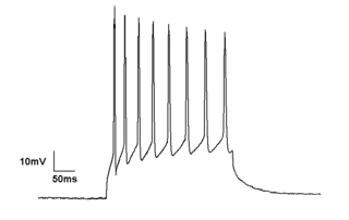
Electrophysiology is the branch of physiology that studies the electrical properties of biological cells and tissues. It involves measurements of voltage changes or electric current or manipulations on a wide variety of scales from single ion channel proteins to whole organs like the heart. In neuroscience, it includes measurements of the electrical activity of neurons, and, in particular, action potential activity. Recordings of large-scale electric signals from the nervous system, such as electroencephalography, may also be referred to as electrophysiological recordings. They are useful for electrodiagnosis and monitoring.

<span class="mw-page-title-main">Atomic force microscopy</span> Type of microscopy

Atomic force microscopy (AFM) or scanning force microscopy (SFM) is a very-high-resolution type of scanning probe microscopy (SPM), with demonstrated resolution on the order of fractions of a nanometer, more than 1000 times better than the optical diffraction limit.

<span class="mw-page-title-main">Patch clamp</span> Laboratory technique in electrophysiology

The patch clamp technique is a laboratory technique in electrophysiology used to study ionic currents in individual isolated living cells, tissue sections, or patches of cell membrane. The technique is especially useful in the study of excitable cells such as neurons, cardiomyocytes, muscle fibers, and pancreatic beta cells, and can also be applied to the study of bacterial ion channels in specially prepared giant spheroplasts.

Scanning probe microscopy (SPM) is a branch of microscopy that forms images of surfaces using a physical probe that scans the specimen. SPM was founded in 1981, with the invention of the scanning tunneling microscope, an instrument for imaging surfaces at the atomic level. The first successful scanning tunneling microscope experiment was done by Gerd Binnig and Heinrich Rohrer. The key to their success was using a feedback loop to regulate gap distance between the sample and the probe.

<span class="mw-page-title-main">Kelvin probe force microscope</span> Noncontact variant of atomic force microscopy

Kelvin probe force microscopy (KPFM), also known as surface potential microscopy, is a noncontact variant of atomic force microscopy (AFM). By raster scanning in the x,y plane the work function of the sample can be locally mapped for correlation with sample features. When there is little or no magnification, this approach can be described as using a scanning Kelvin probe (SKP). These techniques are predominantly used to measure corrosion and coatings.

Nanoelectrochemistry is a branch of electrochemistry that investigates the electrical and electrochemical properties of materials at the nanometer size regime. Nanoelectrochemistry plays significant role in the fabrication of various sensors, and devices for detecting molecules at very low concentrations.

<span class="mw-page-title-main">Focused ion beam</span> Device

Focused ion beam, also known as FIB, is a technique used particularly in the semiconductor industry, materials science and increasingly in the biological field for site-specific analysis, deposition, and ablation of materials. A FIB setup is a scientific instrument that resembles a scanning electron microscope (SEM). However, while the SEM uses a focused beam of electrons to image the sample in the chamber, a FIB setup uses a focused beam of ions instead. FIB can also be incorporated in a system with both electron and ion beam columns, allowing the same feature to be investigated using either of the beams. FIB should not be confused with using a beam of focused ions for direct write lithography. These are generally quite different systems where the material is modified by other mechanisms.

Photothermal microspectroscopy (PTMS), alternatively known as photothermal temperature fluctuation (PTTF), is derived from two parent instrumental techniques: infrared spectroscopy and atomic force microscopy (AFM). In one particular type of AFM, known as scanning thermal microscopy (SThM), the imaging probe is a sub-miniature temperature sensor, which may be a thermocouple or a resistance thermometer. This same type of detector is employed in a PTMS instrument, enabling it to provide AFM/SThM images: However, the chief additional use of PTMS is to yield infrared spectra from sample regions below a micrometer, as outlined below.

<span class="mw-page-title-main">Scanning thermal microscopy</span>

Scanning thermal microscopy (SThM) is a type of scanning probe microscopy that maps the local temperature and thermal conductivity of an interface. The probe in a scanning thermal microscope is sensitive to local temperatures – providing a nano-scale thermometer. Thermal measurements at the nanometer scale are of both scientific and industrial interest. The technique was invented by Clayton C. Williams and H. Kumar Wickramasinghe in 1986.
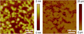
<span class="mw-page-title-main">Photoconductive atomic force microscopy</span> Type of atomic force microscopy

Photoconductive atomic force microscopy (PC-AFM) is a variant of atomic force microscopy that measures photoconductivity in addition to surface forces.

Scanning electrochemical microscopy (SECM) is a technique within the broader class of scanning probe microscopy (SPM) that is used to measure the local electrochemical behavior of liquid/solid, liquid/gas and liquid/liquid interfaces. Initial characterization of the technique was credited to University of Texas electrochemist, Allen J. Bard, in 1989. Since then, the theoretical underpinnings have matured to allow widespread use of the technique in chemistry, biology and materials science. Spatially resolved electrochemical signals can be acquired by measuring the current at an ultramicroelectrode (UME) tip as a function of precise tip position over a substrate region of interest. Interpretation of the SECM signal is based on the concept of diffusion-limited current. Two-dimensional raster scan information can be compiled to generate images of surface reactivity and chemical kinetics.

<span class="mw-page-title-main">Non-contact atomic force microscopy</span>

Non-contact atomic force microscopy (nc-AFM), also known as dynamic force microscopy (DFM), is a mode of atomic force microscopy, which itself is a type of scanning probe microscopy. In nc-AFM a sharp probe is moved close to the surface under study, the probe is then raster scanned across the surface, the image is then constructed from the force interactions during the scan. The probe is connected to a resonator, usually a silicon cantilever or a quartz crystal resonator. During measurements the sensor is driven so that it oscillates. The force interactions are measured either by measuring the change in amplitude of the oscillation at a constant frequency just off resonance or by measuring the change in resonant frequency directly using a feedback circuit to always drive the sensor on resonance.

Sir David Klenerman is a British biophysical chemist and a professor of biophysical chemistry at the Department of Chemistry at the University of Cambridge and a Fellow of Christ's College, Cambridge.

The operation of a photon scanning tunneling microscope (PSTM) is analogous to the operation of an electron scanning tunneling microscope, with the primary distinction being that PSTM involves tunneling of photons instead of electrons from the sample surface to the probe tip. A beam of light is focused on a prism at an angle greater than the critical angle of the refractive medium in order to induce total internal reflection within the prism. Although the beam of light is not propagated through the surface of the refractive prism under total internal reflection, an evanescent field of light is still present at the surface.

A probe tip is an instrument used in scanning probe microscopes (SPMs) to scan the surface of a sample and make nano-scale images of surfaces and structures. The probe tip is mounted on the end of a cantilever and can be as sharp as a single atom. In microscopy, probe tip geometry and the composition of both the tip and the surface being probed directly affect resolution and imaging quality. Tip size and shape are extremely important in monitoring and detecting interactions between surfaces. SPMs can precisely measure electrostatic forces, magnetic forces, chemical bonding, Van der Waals forces, and capillary forces. SPMs can also reveal the morphology and topography of a surface.

Electrochemical AFM (EC-AFM) is a particular type of Scanning probe microscopy (SPM), which combines the classical Atomic force microscopy (AFM) together with electrochemical measurements. EC-AFM allows to perform in-situ AFM measurements in an electrochemical cell, in order to investigate the actual changes in the electrode surface morphology during electrochemical reactions. The solid-liquid interface is thus investigated. This technique was developed for the first time in 1996 by Kouzeki et al., who studied amorphous and polycrystalline thin films of Naphthalocyanine on Indium tin oxide in a solution of 0.1 M Potassium chloride (KCl). Unlike the Electrochemical scanning tunneling microscope, previously developed by Itaya and Tomita in 1988, the tip is non-conductive and it is easily steered in a liquid environment.

<span class="mw-page-title-main">Multi-tip scanning tunneling microscopy</span>

Multi-tip scanning tunneling microscopy extends scanning tunneling microscopy (STM) from imaging to dedicated electrical measurements at the nanoscale like a ″multimeter at the nanoscale″. In materials science, nanoscience, and nanotechnology, it is desirable to measure electrical properties at a particular position of the sample. For this purpose, multi-tip STMs in which several tips are operated independently have been developed. Apart from imaging the sample, the tips of a multi-tip STM are used to form contacts to the sample at desired locations and to perform local electrical measurements.

Single-Entity Electrochemistry (SEE) refers to the electroanalysis of an individual unit of interest. A unique feature of SEE is that it unifies multiple different branches of electrochemistry. Single-Entity Electrochemistry pushes the bounds of the field as it can measure entities on a scale of 100 microns to angstroms. Single-Entity Electrochemistry is important because it gives the ability to view how a single molecule, or cell, or "thing" affects the bulk response, and thus the chemistry that might have gone unknown otherwise. The ability to monitor the movement of one electron or ion from one unit to another is valuable, as many vital reactions and mechanisms undergo this process. Electrochemistry is well suited for this measurement due to its incredible sensitivity. Single-Entity Electrochemistry can be used to investigate nanoparticles, wires, vesicles, nanobubbles, nanotubes, cells, and viruses, and other small molecules and ions. Single-entity electrochemistry has been successfully used to determine the size distribution of particles as well as the number of particles present inside a vesicle or other similar structures

References

  1. Hansma PK, Drake B, Marti O, Gould SA, Prater CB (1989). "The scanning ion-conductance microscope". Science. 243 (4891): 641–3. Bibcode:1989Sci...243..641H. doi:10.1126/science.2464851. PMID   2464851.
  2. 1 2 3 4 Shevchuk AI, Frolenkov GI, Sánchez D, James PS, Freedman N, Lab MJ, Jones R, Klenerman D, Korchev YE (2006). "Imaging proteins in membranes of living cells by high-resolution scanning ion conductance microscopy". Angew. Chem. Int. Ed. Engl. 45 (14): 2212–2216. doi:10.1002/anie.200503915. PMID   16506257.
  3. Rheinlaender J, Geisse NA, Proksch R, Schäffer TE (2011). "Comparison of scanning ion conductance microscopy with atomic force microscopy for cell imaging". Langmuir. 27 (2): 697–704. doi:10.1021/la103275y. PMID   21158392.
  4. Clarke RW, Novak P, Zhukov A, Tyler EJ, Cano-Jaimez M, Drews A, Richards O, Volynski K, Bishop C, Klenerman D (2016). "Low Stress Ion Conductance Microscopy of Sub-Cellular Stiffness". Soft Matter. 12 (38): 7953–8. arXiv: 2103.03811 . Bibcode:2016SMat...12.7953C. doi:10.1039/c6sm01106c. PMC   5166566 . PMID   27604678.
  5. 1 2 Happel, P.; Wehner, F.; Dietzel, I.D. Scanning ion conductance microscopy–a tool to investigate electrolyte-nonconductor interfaces. In Modern Research and Educational Topics in Microscopy; FORMATEX: Badajoz, Spain, 2007; pp. 968–975.
  6. 1 2 Chen CC, Zhou Y, Baker LA (2012). "Scanning ion conductance microscopy". Annual Review of Analytical Chemistry. 5: 207–228. Bibcode:2012ARAC....5..207C. doi:10.1146/annurev-anchem-062011-143203. PMID   22524219.
  7. Rheinlaender J, Schäffer TE (2009). "Image formation, resolution, and height measurement in scanning ion conductance microscopy". J. Appl. Phys. 105 (9): 094905–094905–9. Bibcode:2009JAP...105i4905R. doi:10.1063/1.3122007.
  8. 1 2 3 Gorelik J, Shevchuk AI, Frolenkov GI, Diakonov IA, Lab MJ, Kros CJ, Richardson GP, Vodyanoy I, Edwards CR, Klenerman D, et al. (2003). "Dynamic assembly of surface structures in living cells". Proc. Natl. Acad. Sci. USA. 100 (10): 5819–5822. Bibcode:2003PNAS..100.5819G. doi: 10.1073/pnas.1030502100 . PMC   156284 . PMID   12721367.
  9. 1 2 Gorelik J, Zhang Y, Shevchuk AI, Frolenkov GI, Sánchez D, Lab MJ, Vodyanoy I, Edwards CR, Klenerman D, Korchev YE (2004). "The use of scanning ion conductance microscopy to image A6 cells". Mol. Cell. Endocrinol. 217 (1–2): 101–108. doi:10.1016/j.mce.2003.10.015. PMID   15134807. S2CID   12947242.
  10. 1 2 Zhang Y, Gorelik J, Sanchez D, Shevchuk A, Lab M, Vodyanoy I, Klenerman D, Edwards C, Korchev Y (2005). "Scanning ion conductance microscopy reveals how a functional renal epithelial monolayer maintains its integrity". Kidney Int. 68 (3): 1071–1077. doi: 10.1111/j.1523-1755.2005.00499.x . PMID   16105037.
  11. Mann SA, Hoffmann G, Hengstenberg A, Schuhmann W, Dietzel ID (2002). "Pulse-mode scanning ion conductance microscopy—A method to investigate cultured hippocampal cells". J. Neurosci. Methods. 116 (2): 113–117. doi:10.1016/s0165-0270(02)00023-7. PMID   12044660. S2CID   37799827.
  12. Novak P, Li C, Shevchuk AI, Stepanyan R, Caldwell M, Hughes S, Smart TG, Gorelik J, Ostanin VP, Lab MJ, et al. (2009). "Nanoscale live-cell imaging using hopping probe ion conductance microscopy". Nat. Methods. 6 (4): 279–281. doi:10.1038/nmeth.1306. PMC   2702483 . PMID   19252505.
  13. Nikolaev VO, Moshkov A, Lyon AR, Miragoli M, Novak P, Paur H, Lohse MJ, Korchev YE, Harding SE, Gorelik J (2010). "Beta2-adrenergic receptor redistribution in heart failure changes cAMP compartmentation". Science. 327 (5973): 1653–1657. Bibcode:2010Sci...327.1653N. doi:10.1126/science.1185988. PMID   20185685. S2CID   8227170.
  14. Duclohier H (2005). "Neuronal sodium channels in ventricular heart cells are localized near T-tubules openings". Biochem. Biophys. Res. Commun. 334 (4): 1135–1140. doi:10.1016/j.bbrc.2005.06.203. PMID   16038878.
  15. Proksch R, Lal R, Hansma PK, Morse D, Stucky G (1996). "Imaging the internal and external pore structure of membranes in fluid: TappingMode scanning ion conductance microscopy". Biophysical Journal. 71 (4): 2155–7. Bibcode:1996BpJ....71.2155P. doi:10.1016/s0006-3495(96)79416-x. PMC   1233683 . PMID   8889191.
  16. Bruckbauer A, Ying L, Rothery AM, Korchev YE, Klenerman D (2002). "Characterization of a Novel Light Source for Simultaneous Optical and Scanning Ion Conductance Microscopy". Analytical Chemistry. 74 (11): 2612–2616. doi:10.1021/ac011257y. PMID   12069246.
  17. Rothery AM, Gorelik J, Bruckbauer A, Korchev YE, Klenermann D (2003). "A novel light source for SICM-SNOM of living cells". Journal of Microscopy. 209 (2): 94–101. doi:10.1046/j.1365-2818.2003.01122.x. PMID   12588526. S2CID   10121265.
  18. Zhukov A, Richards O, Ostanin V, Korchev Y, Klenerman D (2012). "A hybrid scanning mode for fast scanning ion conductance microscopy (SICM) imaging". Ultramicroscopy. 121C (11): 1–7. doi:10.1016/j.ultramic.2012.06.015. PMC   3462995 . PMID   22902298.