Related Research Articles

A scanning tunneling microscope (STM) is a type of scanning probe microscope used for imaging surfaces at the atomic level. Its development in 1981 earned its inventors, Gerd Binnig and Heinrich Rohrer, then at IBM Zürich, the Nobel Prize in Physics in 1986. STM senses the surface by using an extremely sharp conducting tip that can distinguish features smaller than 0.1 nm with a 0.01 nm (10 pm) depth resolution. This means that individual atoms can routinely be imaged and manipulated. Most scanning tunneling microscopes are built for use in ultra-high vacuum at temperatures approaching absolute zero, but variants exist for studies in air, water and other environments, and for temperatures over 1000 °C.
In solid-state physics, the work function is the minimum thermodynamic work needed to remove an electron from a solid to a point in the vacuum immediately outside the solid surface. Here "immediately" means that the final electron position is far from the surface on the atomic scale, but still too close to the solid to be influenced by ambient electric fields in the vacuum. The work function is not a characteristic of a bulk material, but rather a property of the surface of the material.

Thermionic emission is the liberation of charged particles from a hot electrode whose thermal energy gives some particles enough kinetic energy to escape the material's surface. The particles, sometimes called thermions in early literature, are now known to be ions or electrons. Thermal electron emission specifically refers to emission of electrons and occurs when thermal energy overcomes the material's work function.

Walter Hans Schottky was a German physicist who played a major early role in developing the theory of electron and ion emission phenomena, invented the screen-grid vacuum tube in 1915 while working at Siemens, co-invented the ribbon microphone and ribbon loudspeaker along with Dr. Erwin Gerlach in 1924 and later made many significant contributions in the areas of semiconductor devices, technical physics and technology.
Field electron emission, also known as field emission (FE) and electron field emission, is emission of electrons induced by an electrostatic field. The most common context is field emission from a solid surface into a vacuum. However, field emission can take place from solid or liquid surfaces, into a vacuum, a fluid, or any non-conducting or weakly conducting dielectric. The field-induced promotion of electrons from the valence to conduction band of semiconductors can also be regarded as a form of field emission. The terminology is historical because related phenomena of surface photoeffect, thermionic emission and "cold electronic emission", i.e. the emission of electrons in strong static electric fields, were discovered and studied independently from the 1880s to 1930s. When the term field emission is used without qualifiers, it typically means "cold emission".

A Schottky barrier, named after Walter H. Schottky, is a potential energy barrier for electrons formed at a metal–semiconductor junction. Schottky barriers have rectifying characteristics, suitable for use as a diode. One of the primary characteristics of a Schottky barrier is the Schottky barrier height, denoted by ΦB. The value of ΦB depends on the combination of metal and semiconductor.
Scanning probe microscopy (SPM) is a branch of microscopy that forms images of surfaces using a physical probe that scans the specimen. SPM was founded in 1981, with the invention of the scanning tunneling microscope, an instrument for imaging surfaces at the atomic level. The first successful scanning tunneling microscope experiment was done by Gerd Binnig and Heinrich Rohrer. The key to their success was using a feedback loop to regulate gap distance between the sample and the probe.
Scanning tunneling spectroscopy (STS), an extension of scanning tunneling microscopy (STM), is used to provide information about the density of electrons in a sample as a function of their energy.

The Schottky effect or field enhanced thermionic emission is a phenomenon in condensed matter physics named after Walter H. Schottky. In electron emission devices, especially electron guns, the thermionic electron emitter will be biased negative relative to its surroundings. This creates an electric field of magnitude F at the emitter surface. Without the field, the surface barrier seen by an escaping Fermi-level electron has height W equal to the local work-function. The electric field lowers the surface barrier by an amount ΔW, and increases the emission current. It can be modeled by a simple modification of the Richardson equation, by replacing W by (W − ΔW). This gives the equation
Spin-polarized scanning tunneling microscopy (SP-STM) is a type of scanning tunneling microscope (STM) that can provide detailed information of magnetic phenomena on the single-atom scale additional to the atomic topography gained with STM. SP-STM opened a novel approach to static and dynamic magnetic processes as precise investigations of domain walls in ferromagnetic and antiferromagnetic systems, as well as thermal and current-induced switching of nanomagnetic particles.

Nanometrology is a subfield of metrology, concerned with the science of measurement at the nanoscale level. Nanometrology has a crucial role in order to produce nanomaterials and devices with a high degree of accuracy and reliability in nanomanufacturing.
In electronics, a tunnel junction is a barrier, such as a thin insulating layer or electric potential, between two electrically conducting materials. Electrons pass through the barrier by the process of quantum tunnelling. Classically, the electron has zero probability of passing through the barrier. However, according to quantum mechanics, the electron has a non-zero wave amplitude in the barrier, and hence it has some probability of passing through the barrier. Tunnel junctions serve a variety of different purposes.
In solid-state physics, a metal–semiconductor (M–S) junction is a type of electrical junction in which a metal comes in close contact with a semiconductor material. It is the oldest type of practical semiconductor device. M–S junctions can either be rectifying or non-rectifying. The rectifying metal–semiconductor junction forms a Schottky barrier, making a device known as a Schottky diode, while the non-rectifying junction is called an ohmic contact.
An optical rectenna is a rectenna that works with visible or infrared light. A rectenna is a circuit containing an antenna and a diode, which turns electromagnetic waves into direct current electricity. While rectennas have long been used for radio waves or microwaves, an optical rectenna would operate the same way but with infrared or visible light, turning it into electricity.
Metal–insulator–metal (MIM) diode is a type of nonlinear device very similar to a semiconductor diode and capable of very fast operation. Depending on the geometry and the material used for fabrication, the operation mechanisms are governed either by quantum tunnelling or thermal activation.
Quantum microscopy allows microscopic properties of matter and quantum particles to be measured and imaged. Various types of microscopy use quantum principles. The first microscope to do so was the scanning tunneling microscope, which paved the way for development of the photoionization microscope and the quantum entanglement microscope.

In a basic Schottky-junction (Schottky-barrier) solar cell, an interface between a metal and a semiconductor provides the band bending necessary for charge separation. Traditional solar cells are composed of p-type and n-type semiconductor layers sandwiched together, forming the source of built-in voltage. Due to differing energy levels between the Fermi level of the metal and the conduction band of the semiconductor, an abrupt potential difference is created, instead of the smooth band transition observed across a p-n junction in a standard solar cell, and this is a Schottky height barrier. Although vulnerable to higher rates of thermionic emission, manufacturing of Schottky barrier solar cells proves to be cost-effective and industrially scalable.
A probe tip is an instrument used in scanning probe microscopes (SPMs) to scan the surface of a sample and make nano-scale images of surfaces and structures. The probe tip is mounted on the end of a cantilever and can be as sharp as a single atom. In microscopy, probe tip geometry and the composition of both the tip and the surface being probed directly affect resolution and imaging quality. Tip size and shape are extremely important in monitoring and detecting interactions between surfaces. SPMs can precisely measure electrostatic forces, magnetic forces, chemical bonding, Van der Waals forces, and capillary forces. SPMs can also reveal the morphology and topography of a surface.
Geometric diodes, also known as morphological diodes, use the shape of their structure and ballistic / quasi-ballistic electron transport to create diode behavior. Geometric diodes differ from all other forms of diodes because they do not rely on a depletion region or a potential barrier to create their diode behavior. Instead of a potential barrier, an asymmetry in the geometry of the material creates an asymmetry in forward vs reverse bias current.
A Ferroelectric tunnel junction (FTJ) is a form of tunnel junction including a ferroelectric dielectric material sandwiched between two electrically conducting materials. Electrons do not directly pass through the junction, and instead they pass the barrier via quantum tunnelling. The structure is similar to a ferroelectric capacitor, but the ferroelectric layer is fabricated thin enough to enable significant tunneling current. The magnitude of the tunneling current is switched by the ferroelectric polarization and is governed by the tunneling electroresistance (TER).
References
- ↑ Haggerty, James J. (1995). Spinoff 1994 (PDF). Washington, D.C.: National Aeronautics and Space Administration, Office of Space Access and Technology, Commercial Development and Technology Transfer Division. ISBN 0-16-045368-2. OCLC 664389243.
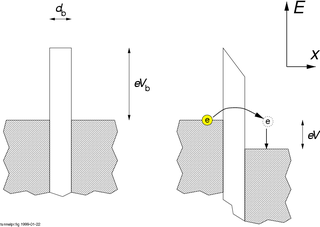
- ↑ Kaiser, W.; Bell, L. (1988). "Direct investigation of subsurface interface electronic structure by ballistic-electron-emission microscopy". Physical Review Letters. 60 (14): 1406–1409. Bibcode:1988PhRvL..60.1406K. doi:10.1103/PhysRevLett.60.1406. PMID 10038030.
- ↑ Bell, L. D.; Kaiser, W. J. (1996). "Ballistic-Electron-Emission Microscopy: A Nanometer-Scale Probe of Interfaces and Carrier Transport". Annual Review of Materials Science . 26: 189–222. Bibcode:1996AnRMS..26..189B. doi:10.1146/annurev.ms.26.080196.001201.
- ↑ Coratger, R.; Ajustron, F. O.; Beauvillain, J. (1994). "Characterization of the metal-semiconductor interface by ballistic electron emission microscopy". Microscopy Microanalysis Microstructures. 5: 31–40. doi: 10.1051/mmm:019940050103100 .

| Authority control databases: National |
|---|