
Atomic force microscopy (AFM) or scanning force microscopy (SFM) is a very-high-resolution type of scanning probe microscopy (SPM), with demonstrated resolution on the order of fractions of a nanometer, more than 1000 times better than the optical diffraction limit.
Scanning probe microscopy (SPM) is a branch of microscopy that forms images of surfaces using a physical probe that scans the specimen. SPM was founded in 1981, with the invention of the scanning tunneling microscope, an instrument for imaging surfaces at the atomic level. The first successful scanning tunneling microscope experiment was done by Gerd Binnig and Heinrich Rohrer. The key to their success was using a feedback loop to regulate gap distance between the sample and the probe.

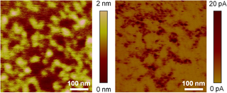
Magnetic force microscopy (MFM) is a variety of atomic force microscopy, in which a sharp magnetized tip scans a magnetic sample; the tip-sample magnetic interactions are detected and used to reconstruct the magnetic structure of the sample surface. Many kinds of magnetic interactions are measured by MFM, including magnetic dipole–dipole interaction. MFM scanning often uses non-contact atomic force microscopy (NC-AFM) and is considered to be non-destructive with respect to the test sample. In MFM, the test sample(s) do not need to be electrically conductive to be imaged.

Kelvin probe force microscopy (KPFM), also known as surface potential microscopy, is a noncontact variant of atomic force microscopy (AFM). By raster scanning in the x,y plane the work function of the sample can be locally mapped for correlation with sample features. When there is little or no magnification, this approach can be described as using a scanning Kelvin probe (SKP). These techniques are predominantly used to measure corrosion and coatings.
Nanotribology is the branch of tribology that studies friction, wear, adhesion and lubrication phenomena at the nanoscale, where atomic interactions and quantum effects are not negligible. The aim of this discipline is characterizing and modifying surfaces for both scientific and technological purposes.
Scanning capacitance microscopy (SCM) is a variety of scanning probe microscopy in which a narrow probe electrode is positioned in contact or close proximity of a sample's surface and scanned. SCM characterizes the surface of the sample using information obtained from the change in electrostatic capacitance between the surface and the probe.

In materials science, chemical force microscopy (CFM) is a variation of atomic force microscopy (AFM) which has become a versatile tool for characterization of materials surfaces. With AFM, structural morphology is probed using simple tapping or contact modes that utilize van der Waals interactions between tip and sample to maintain a constant probe deflection amplitude or maintain height while measuring tip deflection. CFM, on the other hand, uses chemical interactions between functionalized probe tip and sample. Choice chemistry is typically gold-coated tip and surface with R−SH thiols attached, R being the functional groups of interest. CFM enables the ability to determine the chemical nature of surfaces, irrespective of their specific morphology, and facilitates studies of basic chemical bonding enthalpy and surface energy. Typically, CFM is limited by thermal vibrations within the cantilever holding the probe. This limits force measurement resolution to ~1 pN, which is still very suitable considering weak COOH/CH3 interactions are ~20 pN per pair. Hydrophobicity is used as the primary example throughout this consideration of CFM, but certainly any type of bonding can be probed with this method.
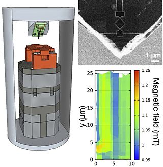
In condensed matter physics, scanning SQUID microscopy is a technique where a superconducting quantum interference device (SQUID) is used to image surface magnetic field strength with micrometre-scale resolution. A tiny SQUID is mounted onto a tip which is then rastered near the surface of the sample to be measured. As the SQUID is the most sensitive detector of magnetic fields available and can be constructed at submicrometre widths via lithography, the scanning SQUID microscope allows magnetic fields to be measured with unparalleled resolution and sensitivity. The first scanning SQUID microscope was built in 1992 by Black et al. Since then the technique has been used to confirm unconventional superconductivity in several high-temperature superconductors including YBCO and BSCCO compounds.

Local oxidation nanolithography (LON) is a tip-based nanofabrication method. It is based on the spatial confinement on an oxidation reaction under the sharp tip of an atomic force microscope.
In microscopy, conductive atomic force microscopy (C-AFM) or current sensing atomic force microscopy (CS-AFM) is a mode in atomic force microscopy (AFM) that simultaneously measures the topography of a material and the electric current flow at the contact point of the tip with the surface of the sample. The topography is measured by detecting the deflection of the cantilever using an optical system, while the current is detected using a current-to-voltage preamplifier. The fact that the CAFM uses two different detection systems is a strong advantage compared to scanning tunneling microscopy (STM). Basically, in STM the topography picture is constructed based on the current flowing between the tip and the sample. Therefore, when a portion of a sample is scanned with an STM, it is not possible to discern if the current fluctuations are related to a change in the topography or to a change in the sample conductivity.

Piezoresponse force microscopy (PFM) is a variant of atomic force microscopy (AFM) that allows imaging and manipulation of piezoelectric/ferroelectric materials domains. This is achieved by bringing a sharp conductive probe into contact with a ferroelectric surface and applying an alternating current (AC) bias to the probe tip in order to excite deformation of the sample through the converse piezoelectric effect (CPE). The resulting deflection of the probe cantilever is detected through standard split photodiode detector methods and then demodulated by use of a lock-in amplifier (LiA). In this way topography and ferroelectric domains can be imaged simultaneously with high resolution.
In microscopy, scanning joule expansion microscopy (SJEM) is a form of scanning probe microscopy heavily based on atomic force microscopy (AFM) that maps the temperature distribution along a surface. Resolutions down to 10 nm have been achieved and 1 nm resolution is theoretically possible. Thermal measurements at the nanometer scale are of both academic and industrial interest, particularly in regards to nanomaterials and modern integrated circuits.

Photoconductive atomic force microscopy (PC-AFM) is a variant of atomic force microscopy that measures photoconductivity in addition to surface forces.
The technique of vibrational analysis with scanning probe microscopy allows probing vibrational properties of materials at the submicrometer scale, and even of individual molecules. This is accomplished by integrating scanning probe microscopy (SPM) and vibrational spectroscopy. This combination allows for much higher spatial resolution than can be achieved with conventional Raman/FTIR instrumentation. The technique is also nondestructive, requires non-extensive sample preparation, and provides more contrast such as intensity contrast, polarization contrast and wavelength contrast, as well as providing specific chemical information and topography images simultaneously.
Nanosensors Inc. is a company that manufactures probes for use in atomic force microscopes (AFM) and scanning probe microscopes (SPM). This private, for profit company was founded November 21, 2018. Nanosensors Inc. is located in Neuchatel, Switzerland.

The colloidal probe technique is commonly used to measure interaction forces acting between colloidal particles and/or planar surfaces in air or in solution. This technique relies on the use of an atomic force microscope (AFM). However, instead of a cantilever with a sharp AFM tip, one uses the colloidal probe. The colloidal probe consists of a colloidal particle of few micrometers in diameter that is attached to an AFM cantilever. The colloidal probe technique can be used in the sphere-plane or sphere-sphere geometries. One typically achieves a force resolution between 1 and 100 pN and a distance resolution between 0.5 and 2 nm.

Non-contact atomic force microscopy (nc-AFM), also known as dynamic force microscopy (DFM), is a mode of atomic force microscopy, which itself is a type of scanning probe microscopy. In nc-AFM a sharp probe is moved close to the surface under study, the probe is then raster scanned across the surface, the image is then constructed from the force interactions during the scan. The probe is connected to a resonator, usually a silicon cantilever or a quartz crystal resonator. During measurements the sensor is driven so that it oscillates. The force interactions are measured either by measuring the change in amplitude of the oscillation at a constant frequency just off resonance or by measuring the change in resonant frequency directly using a feedback circuit to always drive the sensor on resonance.
Nanoprobing is method of extracting device electrical parameters through the use of nanoscale tungsten wires, used primarily in the semiconductor industry. The characterization of individual devices is instrumental to engineers and integrated circuit designers during initial product development and debug. It is commonly utilized in device failure analysis laboratories to aid with yield enhancement, quality and reliability issues and customer returns. Commercially available nanoprobing systems are integrated into either a vacuum-based scanning electron microscope (SEM) or atomic force microscope (AFM). Nanoprobing systems that are based on AFM technology are referred to as Atomic Force nanoProbers (AFP).
The operation of a photon scanning tunneling microscope (PSTM) is analogous to the operation of an electron scanning tunneling microscope, with the primary distinction being that PSTM involves tunneling of photons instead of electrons from the sample surface to the probe tip. A beam of light is focused on a prism at an angle greater than the critical angle of the refractive medium in order to induce total internal reflection within the prism. Although the beam of light is not propagated through the surface of the refractive prism under total internal reflection, an evanescent field of light is still present at the surface.
A probe tip is an instrument used in scanning probe microscopes (SPMs) to scan the surface of a sample and make nano-scale images of surfaces and structures. The probe tip is mounted on the end of a cantilever and can be as sharp as a single atom. In microscopy, probe tip geometry and the composition of both the tip and the surface being probed directly affect resolution and imaging quality. Tip size and shape are extremely important in monitoring and detecting interactions between surfaces. SPMs can precisely measure electrostatic forces, magnetic forces, chemical bonding, Van der Waals forces, and capillary forces. SPMs can also reveal the morphology and topography of a surface.

