Related Research Articles

Atomic force microscopy (AFM) or scanning force microscopy (SFM) is a very-high-resolution type of scanning probe microscopy (SPM), with demonstrated resolution on the order of fractions of a nanometer, more than 1000 times better than the optical diffraction limit.
Scanning probe microscopy (SPM) is a branch of microscopy that forms images of surfaces using a physical probe that scans the specimen. SPM was founded in 1981, with the invention of the scanning tunneling microscope, an instrument for imaging surfaces at the atomic level. The first successful scanning tunneling microscope experiment was done by Gerd Binnig and Heinrich Rohrer. The key to their success was using a feedback loop to regulate gap distance between the sample and the probe.

A scanning transmission electron microscope (STEM) is a type of transmission electron microscope (TEM). Pronunciation is [stɛm] or [ɛsti:i:ɛm]. As with a conventional transmission electron microscope (CTEM), images are formed by electrons passing through a sufficiently thin specimen. However, unlike CTEM, in STEM the electron beam is focused to a fine spot which is then scanned over the sample in a raster illumination system constructed so that the sample is illuminated at each point with the beam parallel to the optical axis. The rastering of the beam across the sample makes STEM suitable for analytical techniques such as Z-contrast annular dark-field imaging, and spectroscopic mapping by energy dispersive X-ray (EDX) spectroscopy, or electron energy loss spectroscopy (EELS). These signals can be obtained simultaneously, allowing direct correlation of images and spectroscopic data.

Magnetic force microscopy (MFM) is a variety of atomic force microscopy, in which a sharp magnetized tip scans a magnetic sample; the tip-sample magnetic interactions are detected and used to reconstruct the magnetic structure of the sample surface. Many kinds of magnetic interactions are measured by MFM, including magnetic dipole–dipole interaction. MFM scanning often uses non-contact AFM (NC-AFM) mode.

Focused ion beam, also known as FIB, is a technique used particularly in the semiconductor industry, materials science and increasingly in the biological field for site-specific analysis, deposition, and ablation of materials. A FIB setup is a scientific instrument that resembles a scanning electron microscope (SEM). However, while the SEM uses a focused beam of electrons to image the sample in the chamber, a FIB setup uses a focused beam of ions instead. FIB can also be incorporated in a system with both electron and ion beam columns, allowing the same feature to be investigated using either of the beams. FIB should not be confused with using a beam of focused ions for direct write lithography. These are generally quite different systems where the material is modified by other mechanisms.

Near-field scanning optical microscopy (NSOM) or scanning near-field optical microscopy (SNOM) is a microscopy technique for nanostructure investigation that breaks the far field resolution limit by exploiting the properties of evanescent waves. In SNOM, the excitation laser light is focused through an aperture with a diameter smaller than the excitation wavelength, resulting in an evanescent field on the far side of the aperture. When the sample is scanned at a small distance below the aperture, the optical resolution of transmitted or reflected light is limited only by the diameter of the aperture. In particular, lateral resolution of 6 nm and vertical resolution of 2–5 nm have been demonstrated.

Magnetic resonance microscopy is magnetic resonance imaging (MRI) at a microscopic level down to the scale of microns. The first definition of MRM was MRI having voxel resolutions of better than 100 μm.
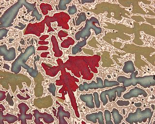
Characterization, when used in materials science, refers to the broad and general process by which a material's structure and properties are probed and measured. It is a fundamental process in the field of materials science, without which no scientific understanding of engineering materials could be ascertained. The scope of the term often differs; some definitions limit the term's use to techniques which study the microscopic structure and properties of materials, while others use the term to refer to any materials analysis process including macroscopic techniques such as mechanical testing, thermal analysis and density calculation. The scale of the structures observed in materials characterization ranges from angstroms, such as in the imaging of individual atoms and chemical bonds, up to centimeters, such as in the imaging of coarse grain structures in metals.
Spin-polarized scanning tunneling microscopy (SP-STM) is a type of scanning tunneling microscope (STM) that can provide detailed information of magnetic phenomena on the single-atom scale additional to the atomic topography gained with STM. SP-STM opened a novel approach to static and dynamic magnetic processes as precise investigations of domain walls in ferromagnetic and antiferromagnetic systems, as well as thermal and current-induced switching of nanomagnetic particles.
Magnetic resonance can mean:

Scanning thermal microscopy (SThM) is a type of scanning probe microscopy that maps the local temperature and thermal conductivity of an interface. The probe in a scanning thermal microscope is sensitive to local temperatures – providing a nano-scale thermometer. Thermal measurements at the nanometer scale are of both scientific and industrial interest. The technique was invented by Clayton C. Williams and H. Kumar Wickramasinghe in 1986.
Spinmechatronics is neologism referring to an emerging field of research concerned with the exploitation of spin-dependent phenomena and established spintronic methodologies and technologies in conjunction with electro-mechanical, magno-mechanical, acousto-mechanical and opto-mechanical systems. Most especially, spinmechatronics concerns the integration of micro- and nano- mechatronic systems with spin physics and spintronics.

Piezoresponse force microscopy (PFM) is a variant of atomic force microscopy (AFM) that allows imaging and manipulation of piezoelectric/ferroelectric materials domains. This is achieved by bringing a sharp conductive probe into contact with a ferroelectric surface and applying an alternating current (AC) bias to the probe tip in order to excite deformation of the sample through the converse piezoelectric effect (CPE). The resulting deflection of the probe cantilever is detected through standard split photodiode detector methods and then demodulated by use of a lock-in amplifier (LiA). In this way topography and ferroelectric domains can be imaged simultaneously with high resolution.
In magnetism, single domain refers to the state of a ferromagnet in which the magnetization does not vary across the magnet. A magnetic particle that stays in a single domain state for all magnetic fields is called a single domain particle. Such particles are very small. They are also very important in a lot of applications because they have a high coercivity. They are the main source of hardness in hard magnets, the carriers of magnetic storage in tape drives, and the best recorders of the ancient Earth's magnetic field.

Thermal scanning probe lithography (t-SPL) is a form of scanning probe lithography (SPL) whereby material is structured on the nanoscale using scanning probes, primarily through the application of thermal energy.
The technique of vibrational analysis with scanning probe microscopy allows probing vibrational properties of materials at the submicrometer scale, and even of individual molecules. This is accomplished by integrating scanning probe microscopy (SPM) and vibrational spectroscopy. This combination allows for much higher spatial resolution than can be achieved with conventional Raman/FTIR instrumentation. The technique is also nondestructive, requires non-extensive sample preparation, and provides more contrast such as intensity contrast, polarization contrast and wavelength contrast, as well as providing specific chemical information and topography images simultaneously.
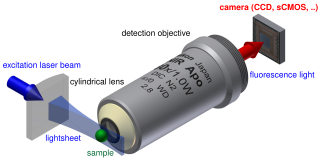
Light sheet fluorescence microscopy (LSFM) is a fluorescence microscopy technique with an intermediate-to-high optical resolution, but good optical sectioning capabilities and high speed. In contrast to epifluorescence microscopy only a thin slice of the sample is illuminated perpendicularly to the direction of observation. For illumination, a laser light-sheet is used, i.e. a laser beam which is focused only in one direction. A second method uses a circular beam scanned in one direction to create the lightsheet. As only the actually observed section is illuminated, this method reduces the photodamage and stress induced on a living sample. Also the good optical sectioning capability reduces the background signal and thus creates images with higher contrast, comparable to confocal microscopy. Because light sheet fluorescence microscopy scans samples by using a plane of light instead of a point, it can acquire images at speeds 100 to 1,000 times faster than those offered by point-scanning methods.

Non-contact atomic force microscopy (nc-AFM), also known as dynamic force microscopy (DFM), is a mode of atomic force microscopy, which itself is a type of scanning probe microscopy. In nc-AFM a sharp probe is moved close to the surface under study, the probe is then raster scanned across the surface, the image is then constructed from the force interactions during the scan. The probe is connected to a resonator, usually a silicon cantilever or a quartz crystal resonator. During measurements the sensor is driven so that it oscillates. The force interactions are measured either by measuring the change in amplitude of the oscillation at a constant frequency just off resonance or by measuring the change in resonant frequency directly using a feedback circuit to always drive the sensor on resonance.
AFM-IR or infrared nanospectroscopy is one of a family of techniques that are derived from a combination of two parent instrumental techniques. AFM-IR combines the chemical analysis power of infrared spectroscopy and the high-spatial resolution of scanning probe microscopy (SPM). The term was first used to denote a method that combined a tuneable free electron laser with an atomic force microscope equipped with a sharp probe that measured the local absorption of infrared light by a sample with nanoscale spatial resolution.
Quantum microscopy allows microscopic properties of matter and quantum particles to be measured and imaged. Various types of microscopy use quantum principles. The first microscope to do so was the scanning tunneling microscope, which paved the way for development of the photoionization microscope and the quantum entanglement microscope.
References
- ↑ J. A. Sidles (1991). "Noninductive detection of single-proton magnetic resonance". Applied Physics Letters. 58 (24): 2854–6. Bibcode:1991ApPhL..58.2854S. doi:10.1063/1.104757.
- ↑ O. Zuger & D. Rugar (1993). "First images from a magnetic resonance force microscope". Applied Physics Letters. 63 (18): 2496–8. Bibcode:1993ApPhL..63.2496Z. doi:10.1063/1.110460.
- ↑ S. Chao; W. Dougherty; J. Garbini; J. Sidles (2003). "Nanometer-scale magnetic resonance imaging". Review of Scientific Instruments. 75 (5): 1175–81. Bibcode:2004RScI...75.1175C. doi:10.1063/1.1666983.
- ↑ D. Rugar; R. Budakian; H. Mamin; B. Chui (2004). "Single spin detection by magnetic resonance force microscopy". Nature. 430 (6997): 329–32. Bibcode:2004Natur.430..329R. doi:10.1038/nature02658. PMID 15254532. S2CID 4346337.
- ↑ C. L. Degen; M. Poggio; H. J. Mamin; C. T. Rettner & D. Rugar (2009). "Nanoscale magnetic resonance imaging". PNAS. 106 (5): 1313–7. Bibcode:2009PNAS..106.1313D. doi: 10.1073/pnas.0812068106 . PMC 2628306 . PMID 19139397.
