This article needs to be updated.(December 2021) |
Computer memory and computer data storage types |
---|
Volatile |
Non-volatile |
Racetrack memory or domain-wall memory (DWM) is an experimental non-volatile memory device under development at IBM's Almaden Research Center by a team led by physicist Stuart Parkin. [1] It is a current topic of active research at the Max Planck Institute of Microstructure Physics in Dr. Parkin's group. In early 2008, a 3-bit version was successfully demonstrated. [2] If it were to be developed successfully, racetrack memory would offer storage density higher than comparable solid-state memory devices like flash memory.[ citation needed ]
Racetrack memory uses a spin-coherent electric current to move magnetic domains along a nanoscopic permalloy wire about 200 nm across and 100 nm thick. As current is passed through the wire, the domains pass by magnetic read/write heads positioned near the wire, which alter the domains to record patterns of bits. A racetrack memory device is made up of many such wires and read/write elements. In general operational concept, racetrack memory is similar to the earlier bubble memory of the 1960s and 1970s. Delay-line memory, such as mercury delay lines of the 1940s and 1950s, are a still-earlier form of similar technology, as used in the UNIVAC and EDSAC computers. Like bubble memory, racetrack memory uses electrical currents to "push" a sequence of magnetic domains through a substrate and past read/write elements. Improvements in magnetic detection capabilities, based on the development of spintronic magnetoresistive sensors, allow the use of much smaller magnetic domains to provide far higher bit densities.
In production, it was expected[ citation needed ] that the wires could be scaled down to around 50 nm. There were two arrangements considered for racetrack memory. The simplest was a series of flat wires arranged in a grid with read and write heads arranged nearby. A more widely studied arrangement used U-shaped wires arranged vertically over a grid of read/write heads on an underlying substrate. This would allow the wires to be much longer without increasing its 2D area, although the need to move individual domains further along the wires before they reach the read/write heads results in slower random access times. Both arrangements offered about the same throughput performance. The primary concern in terms of construction was practical; whether or not the three dimensional vertical arrangement would be feasible to mass-produce.
Projections in 2008 suggested that racetrack memory would offer performance on the order of 20-32 ns to read or write a random bit. This compared to about 10,000,000 ns for a hard drive, or 20-30 ns for conventional DRAM. The primary authors discussed ways to improve the access times with the use of a "reservoir" to about 9.5 ns. Aggregate throughput, with or without the reservoir, would be on the order of 250-670 Mbit/s for racetrack memory, compared to 12800 Mbit/s for a single DDR3 DRAM, 1000 Mbit/s for high-performance hard drives, and 1000 to 4000 Mbit/s for flash memory devices. The only current technology that offered a clear latency benefit over racetrack memory was SRAM, on the order of 0.2 ns, but at a higher cost. Larger feature size "F" of about 45 nm (as of 2011) with a cell area of about 140 F2. [3] [4]
Racetrack memory is one among several emerging technologies that aim to replace conventional memories such as DRAM and Flash, and potentially offer a universal memory device applicable to a wide variety of roles. Other contenders included magnetoresistive random-access memory (MRAM), phase-change memory (PCRAM) and ferroelectric RAM (FeRAM). Most of these technologies offer densities similar to flash memory, in most cases worse, and their primary advantage is the lack of write-endurance limits like those in flash memory. Field-MRAM offers excellent performance as high as 3 ns access time, but requires a large 25-40 F² cell size. It might see use as an SRAM replacement, but not as a mass storage device. The highest densities from any of these devices is offered by PCRAM, with a cell size of about 5.8 F², similar to flash memory, as well as fairly good performance around 50 ns. Nevertheless, none of these can come close to competing with racetrack memory in overall terms, especially density. For example, 50 ns allows about five bits to be operated in a racetrack memory device, resulting in an effective cell size of 20/5=4 F², easily exceeding the performance-density product of PCM. On the other hand, without sacrificing bit density, the same 20 F² area could fit 2.5 2-bit 8 F² alternative memory cells (such as resistive RAM (RRAM) or spin-torque transfer MRAM), each of which individually operating much faster (~10 ns).
In most cases, memory devices store one bit in any given location, so they are typically compared in terms of "cell size", a cell storing one bit. Cell size itself is given in units of F², where "F" is the feature size design rule, representing usually the metal line width. Flash and racetrack both store multiple bits per cell, but the comparison can still be made. For instance, hard drives appeared to be reaching theoretical limits around 650 nm²/bit, [5] defined primarily by the capability to read and write to specific areas of the magnetic surface. DRAM has a cell size of about 6 F², SRAM is much less dense at 120 F². NAND flash memory is currently the densest form of non-volatile memory in widespread use, with a cell size of about 4.5 F², but storing three bits per cell for an effective size of 1.5 F². NOR flash memory is slightly less dense, at an effective 4.75 F², accounting for 2-bit operation on a 9.5 F² cell size. [4] In the vertical orientation (U-shaped) racetrack, nearly 10-20 bits are stored per cell, which itself would have a physical size of at least about 20 F². In addition, bits at different positions on the "track" would take different times (from ~10 to ~1000 ns, or 10 ns/bit) to be accessed by the read/write sensor, because the "track" would move the domains at a fixed rate of ~100 m/s past the read/write sensor.
One limitation of the early experimental devices was that the magnetic domains could be pushed only slowly through the wires, requiring current pulses on the orders of microseconds to move them successfully. This was unexpected, and led to performance equal roughly to that of hard drives, as much as 1000 times slower than predicted. Recent research has traced this problem to microscopic imperfections in the crystal structure of the wires which led to the domains becoming "stuck" at these imperfections. Using an X-ray microscope to directly image the boundaries between the domains, their research found that domain walls would be moved by pulses as short as a few nanoseconds when these imperfections were absent. This corresponds to a macroscopic performance of about 110 m/s. [6]
The voltage required to drive the domains along the racetrack would be proportional to the length of the wire. The current density must be sufficiently high to push the domain walls (as in electromigration). A difficulty for racetrack technology arises from the need for high current density (>108 A/cm2); a 30 nm x 100 nm cross-section would require >3 mA. The resulting power draw becomes higher than that required for other memories, e.g., spin-transfer torque memory (STT-RAM) or flash memory.
Another challenge associated with racetrack memory is the stochastic nature in which the domain walls move, i.e., they move and stop at random positions. [7] There have been attempts to overcome this challenge by producing notches at the edges of the nanowire. [8] Researchers have also proposed staggered nanowires to pin the domain walls precisely. [9] Experimental investigations have shown [10] the effectiveness of staggered domain wall memory. [11] Recently researchers have proposed non-geometrical approaches such as local modulation of magnetic properties through composition modification. Techniques such as annealing induced diffusion [12] and ion-implantation [13] are used.
Computer memory stores information, such as data and programs, for immediate use in the computer. The term memory is often synonymous with the terms RAM,main memory, or primary storage. Archaic synonyms for main memory include core and store.
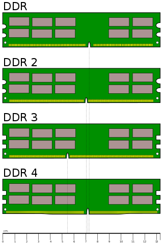
Double Data Rate Synchronous Dynamic Random-Access Memory is a double data rate (DDR) synchronous dynamic random-access memory (SDRAM) class of memory integrated circuits used in computers. DDR SDRAM, also retroactively called DDR1 SDRAM, has been superseded by DDR2 SDRAM, DDR3 SDRAM, DDR4 SDRAM and DDR5 SDRAM. None of its successors are forward or backward compatible with DDR1 SDRAM, meaning DDR2, DDR3, DDR4 and DDR5 memory modules will not work on DDR1-equipped motherboards, and vice versa.
Flash memory is an electronic non-volatile computer memory storage medium that can be electrically erased and reprogrammed. The two main types of flash memory, NOR flash and NAND flash, are named for the NOR and NAND logic gates. Both use the same cell design, consisting of floating gate MOSFETs. They differ at the circuit level depending on whether the state of the bit line or word lines is pulled high or low: in NAND flash, the relationship between the bit line and the word lines resembles a NAND gate; in NOR flash, it resembles a NOR gate.
Static random-access memory is a type of random-access memory (RAM) that uses latching circuitry (flip-flop) to store each bit. SRAM is volatile memory; data is lost when power is removed.
Synchronous dynamic random-access memory is any DRAM where the operation of its external pin interface is coordinated by an externally supplied clock signal.
Bubble memory is a type of non-volatile computer memory that uses a thin film of a magnetic material to hold small magnetized areas, known as bubbles or domains, each storing one bit of data. The material is arranged to form a series of parallel tracks that the bubbles can move along under the action of an external magnetic field. The bubbles are read by moving them to the edge of the material, where they can be read by a conventional magnetic pickup, and then rewritten on the far edge to keep the memory cycling through the material. In operation, bubble memories are similar to delay-line memory systems.
Non-volatile random-access memory (NVRAM) is random-access memory that retains data without applied power. This is in contrast to dynamic random-access memory (DRAM) and static random-access memory (SRAM), which both maintain data only for as long as power is applied, or forms of sequential-access memory such as magnetic tape, which cannot be randomly accessed but which retains data indefinitely without electric power.
Magnetoresistive random-access memory (MRAM) is a type of non-volatile random-access memory which stores data in magnetic domains. Developed in the mid-1980s, proponents have argued that magnetoresistive RAM will eventually surpass competing technologies to become a dominant or even universal memory. Currently, memory technologies in use such as flash RAM and DRAM have practical advantages that have so far kept MRAM in a niche role in the market.
Non-volatile memory (NVM) or non-volatile storage is a type of computer memory that can retain stored information even after power is removed. In contrast, volatile memory needs constant power in order to retain data.
Nano-RAM is a proprietary computer memory technology from the company Nantero. It is a type of nonvolatile random-access memory based on the position of carbon nanotubes deposited on a chip-like substrate. In theory, the small size of the nanotubes allows for very high density memories. Nantero also refers to it as NRAM.
Phase-change memory is a type of non-volatile random-access memory. PRAMs exploit the unique behaviour of chalcogenide glass. In PCM, heat produced by the passage of an electric current through a heating element generally made of titanium nitride is used to either quickly heat and quench the glass, making it amorphous, or to hold it in its crystallization temperature range for some time, thereby switching it to a crystalline state. PCM also has the ability to achieve a number of distinct intermediary states, thereby having the ability to hold multiple bits in a single cell, but the difficulties in programming cells in this way has prevented these capabilities from being implemented in other technologies with the same capability.
Magnetic storage or magnetic recording is the storage of data on a magnetized medium. Magnetic storage uses different patterns of magnetisation in a magnetizable material to store data and is a form of non-volatile memory. The information is accessed using one or more read/write heads.
Density is a measure of the quantity of information bits that can be stored on a given physical space of a computer storage medium. There are three types of density: length of track, area of the surface, or in a given volume.
Millipede memory is a form of non-volatile computer memory. It promised a data density of more than 1 terabit per square inch, which is about the limit of the perpendicular recording hard drives. Millipede storage technology was pursued as a potential replacement for magnetic recording in hard drives and a means of reducing the physical size of the technology to that of flash media.
Ferroelectric RAM is a random-access memory similar in construction to DRAM but using a ferroelectric layer instead of a dielectric layer to achieve non-volatility. FeRAM is one of a growing number of alternative non-volatile random-access memory technologies that offer the same functionality as flash memory. An FeRAM chip contains a thin film of ferroelectric material, often lead zirconate titanate, commonly referred to as PZT. The atoms in the PZT layer change polarity in an electric field, thereby producing a power-efficient binary switch. However, the most important aspect of the PZT is that it is not affected by power disruption or magnetic interference, making FeRAM a reliable nonvolatile memory.
Spin-transfer torque (STT) is an effect in which the orientation of a magnetic layer in a magnetic tunnel junction or spin valve can be modified using a spin-polarized current.
Nanoelectronics refers to the use of nanotechnology in electronic components. The term covers a diverse set of devices and materials, with the common characteristic that they are so small that inter-atomic interactions and quantum mechanical properties need to be studied extensively. Some of these candidates include: hybrid molecular/semiconductor electronics, one-dimensional nanotubes/nanowires or advanced molecular electronics.
Universal memory refers to a computer data storage device combining the cost benefits of DRAM, the speed of SRAM, the non-volatility of flash memory along with infinite durability, and longevity. Such a device, if it ever becomes possible to develop, would have a far-reaching impact on the computer market. Some doubt that such a type of memory will ever be possible.
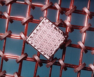
Random-access memory is a form of electronic computer memory that can be read and changed in any order, typically used to store working data and machine code. A random-access memory device allows data items to be read or written in almost the same amount of time irrespective of the physical location of data inside the memory, in contrast with other direct-access data storage media, where the time required to read and write data items varies significantly depending on their physical locations on the recording medium, due to mechanical limitations such as media rotation speeds and arm movement.
Everspin Technologies, Inc. is a publicly traded semiconductor company headquartered in Chandler, Arizona, United States. It develops and manufactures discrete magnetoresistive RAM or magnetoresistive random-access memory (MRAM) products, including Toggle MRAM and Spin-Transfer Torque MRAM (STT-MRAM) product families. It also licenses its technology for use in embedded MRAM (eMRAM) applications, magnetic sensor applications as well as performs backend foundry services for eMRAM.