Electron-beam physical vapor deposition

Last updated

Electron-beam physical vapor deposition, or EBPVD, is a form of physical vapor deposition in which a target anode is bombarded with an electron beam given off by a charged tungsten filament under high vacuum. The electron beam causes atoms from the target to transform into the gaseous phase. These atoms then precipitate into solid form, coating everything in the vacuum chamber (within line of sight) with a thin layer of the anode material.

Contents

Introduction

Thin-film deposition is a process applied in the semiconductor industry to grow electronic materials, in the aerospace industry to form thermal and chemical barrier coatings to protect surfaces against corrosive environments, in optics to impart the desired reflective and transmissive properties to a substrate and elsewhere in industry to modify surfaces to have a variety of desired properties. The deposition process can be broadly classified into physical vapor deposition (PVD) and chemical vapor deposition (CVD). In CVD, the film growth takes place at high temperatures, leading to the formation of corrosive gaseous products, and it may leave impurities in the film. The PVD process can be carried out at lower deposition temperatures and without corrosive products, but deposition rates are typically lower. Electron-beam physical vapor deposition, however, yields a high deposition rate from 0.1 to 100 μm/min at relatively low substrate temperatures, with very high material utilization efficiency. The schematic of an EBPVD system is shown in Fig 1.

Fig 1. Electromagnetic alignment. The ingot is held at a positive potential relative to the filament. To avoid chemical interactions between the filament and the ingot material, the filament is kept out of sight. A magnetic field is employed to direct the electron beam from its source to the ingot location. An additional electric field can be used to steer the beam over the ingot surface allowing uniform heating. Electron Beam Deposition 001.jpg
Fig 1. Electromagnetic alignment. The ingot is held at a positive potential relative to the filament. To avoid chemical interactions between the filament and the ingot material, the filament is kept out of sight. A magnetic field is employed to direct the electron beam from its source to the ingot location. An additional electric field can be used to steer the beam over the ingot surface allowing uniform heating.

Thin-film deposition process

In an EBPVD system, the deposition chamber must be evacuated to a pressure of at least 7.5×10⁻⁵ Torr (10−2 Pa) to allow passage of electrons from the electron gun to the evaporation material, which can be in the form of an ingot or rod. [1] Alternatively, some modern EBPVD systems utilize an arc-suppression system and can be operated at vacuum levels as low as 5.0×10⁻³ Torr, for situations such as parallel use with magnetron sputtering. [2] Multiple types of evaporation materials and electron guns can be used simultaneously in a single EBPVD system, each having a power from tens to hundreds of kilowatts. Electron beams can be generated by thermionic emission, field electron emission or the anodic arc method. The generated electron beam is accelerated to a high kinetic energy and directed towards the evaporation material. Upon striking the evaporation material, the electrons will lose their energy very rapidly. [3] The kinetic energy of the electrons is converted into other forms of energy through interactions with the evaporation material. The thermal energy that is produced heats up the evaporation material causing it to melt or sublimate. Once temperature and vacuum level are sufficiently high, vapor will result from the melt or solid. The resulting vapor can then be used to coat surfaces. Accelerating voltages can be between 3 and 40 kV. When the accelerating voltage is 20–25 kV and the beam current is a few amperes, 85% of the electron's kinetic energy can be converted into thermal energy. Some of the incident electron energy is lost through the production of X-rays and secondary electron emission.

There are three main EBPVD configurations, electromagnetic alignment, electromagnetic focusing and the pendant drop configuration. Electromagnetic alignment and electromagnetic focusing use evaporation material that is in the form of an ingot, while the pendant drop configuration uses a rod. Ingots are enclosed in a copper crucible or hearth, [4] while a rod will be mounted at one end in a socket. Both the crucible and socket must be cooled. This is typically done by water circulation. In the case of ingots, molten liquid can form on its surface, which can be kept constant by vertical displacement of the ingot. The evaporation rate may be on the order of 10−2 g/(cm2·s).

Material evaporation methods

Refractory carbides like titanium carbide and borides like titanium boride and zirconium boride can evaporate without undergoing decomposition in the vapor phase. These compounds are deposited by direct evaporation. In this process these compounds, compacted in the form of an ingot, are evaporated in vacuum by the focused high-energy electron beam, and the vapors are directly condensed over the substrate.

Certain refractory oxides and carbides undergo fragmentation during their evaporation by the electron beam, resulting in a stoichiometry that is different from the initial material. For example, alumina, when evaporated by electron beam, dissociates into aluminum, AlO3 and Al2O. Some refractory carbides like silicon carbide and tungsten carbide decompose upon heating, and the dissociated elements have different volatilities. These compounds can be deposited on the substrate either by reactive evaporation or by co-evaporation. In the reactive evaporation process, the metal is evaporated from the ingot by the electron beam. The vapors are carried by the reactive gas, which is oxygen in case of metal oxides or acetylene in case of metal carbides. When the thermodynamic conditions are met, the vapors react with the gas in the vicinity of the substrate to form films. Metal carbide films can also be deposited by co-evaporation. In this process, two ingots are used, one for metal and the other for carbon. Each ingot is heated with a different beam energy so that their evaporation rate can be controlled. As the vapors arrive at the surface, they chemically combine under proper thermodynamic conditions to form a metal carbide film.

The substrate

The substrate on which the film deposition takes place is ultrasonically cleaned and fastened to the substrate holder. The substrate holder is attached to the manipulator shaft. The manipulator shaft moves translationally to adjust the distance between the ingot source and the substrate. The shaft also rotates the substrate at a particular speed so that the film is uniformly deposited on the substrate. A negative bias DC voltage of 200–400 V can be applied to the substrate. Often, focused high-energy electrons from one of the electron guns or infrared light from heater lamps is used to preheat the substrate. Heating of the substrate allows increased adatom–substrate and adatom–film diffusion by giving the adatoms sufficient energy to overcome kinetic barriers. If a rough film, such as metallic nanorods, [5] is desired substrate cooling with water or liquid nitrogen may be employed to reduce diffusion lifetime, positively bolstering surface kinetic barriers. To further enhance film roughness, the substrate may be mounted at a steep angle with respect to the flux to achieve geometric shadowing, where incoming line of sight flux lands onto only higher parts of the developing film. This method is known as glancing-angle deposition (GLAD) [6] or oblique-angle deposition (OAD). [7]

Ion-beam-assisted deposition

EBPVD systems are equipped with ion sources. These ion sources are used for substrate etching and cleaning, sputtering the target and controlling the microstructure of the substrate. The ion beams bombard the surface and alter the microstructure of the film. When the deposition reaction takes place on the hot substrate surface, the films can develop an internal tensile stress due to the mismatch in the coefficient of thermal expansion between the substrate and the film. High-energy ions can be used to bombard these ceramic thermal barrier coatings and change the tensile stress into compressive stress. Ion bombardment also increases the density of the film, changes the grain size and modifies amorphous films to polycrystalline films. Low-energy ions are used for the surfaces of semiconductor films.

Advantages

The deposition rate in this process can be as low as 1 nm per minute to as high as few micrometers per minute. The material utilization efficiency is high relative to other methods, and the process offers structural and morphological control of films. Due to the very high deposition rate, this process has potential industrial application for wear-resistant and thermal barrier coatings in aerospace industries, hard coatings for cutting and tool industries, and electronic and optical films for semiconductor industries and thin-film solar applications.

Disadvantages

EBPVD is a line-of-sight deposition process when performed at a low enough pressure (roughly <10−4 Torr ). The translational and rotational motion of the shaft helps for coating the outer surface of complex geometries, but this process cannot be used to coat the inner surface of complex geometries. Another potential problem is that filament degradation in the electron gun results in a non-uniform evaporation rate.

However, when vapor deposition is performed at pressures of roughly 10−4 Torr (1.3×10⁻⁴ hPa) or higher, significant scattering of the vapor cloud takes place such that surfaces not in sight of the source can be coated. Strictly speaking, the slow transition from line-of-sight to scattered deposition is determined not only by pressure (or mean free path) but also by source-to-substrate distance.

Certain materials are not well-suited to evaporation by EBPVD. The following reference materials suggest appropriate evaporation techniques for many materials:

Also see Oxford's Evaporation Guide for the Elements.

See also

Related Research Articles

<span class="mw-page-title-main">Chemical vapor deposition</span> Method used to apply surface coatings

Chemical vapor deposition (CVD) is a vacuum deposition method used to produce high-quality, and high-performance, solid materials. The process is often used in the semiconductor industry to produce thin films.

<span class="mw-page-title-main">MEMS</span> Very small devices that incorporate moving components

MEMS is the technology of microscopic devices incorporating both electronic and moving parts. MEMS are made up of components between 1 and 100 micrometres in size, and MEMS devices generally range in size from 20 micrometres to a millimetre, although components arranged in arrays can be more than 1000 mm2. They usually consist of a central unit that processes data and several components that interact with the surroundings.

<span class="mw-page-title-main">Molecular-beam epitaxy</span> Crystal growth process

Molecular-beam epitaxy (MBE) is an epitaxy method for thin-film deposition of single crystals. MBE is widely used in the manufacture of semiconductor devices, including transistors, and it is considered one of the fundamental tools for the development of nanotechnologies. MBE is used to fabricate diodes and MOSFETs at microwave frequencies, and to manufacture the lasers used to read optical discs.

<span class="mw-page-title-main">Pulsed laser deposition</span>

Pulsed laser deposition (PLD) is a physical vapor deposition (PVD) technique where a high-power pulsed laser beam is focused inside a vacuum chamber to strike a target of the material that is to be deposited. This material is vaporized from the target which deposits it as a thin film on a substrate. This process can occur in ultra high vacuum or in the presence of a background gas, such as oxygen which is commonly used when depositing oxides to fully oxygenate the deposited films.

Since the mid-20th century, electron-beam technology has provided the basis for a variety of novel and specialized applications in semiconductor manufacturing, microelectromechanical systems, nanoelectromechanical systems, and microscopy.

A thin film is a layer of material ranging from fractions of a nanometer (monolayer) to several micrometers in thickness. The controlled synthesis of materials as thin films is a fundamental step in many applications. A familiar example is the household mirror, which typically has a thin metal coating on the back of a sheet of glass to form a reflective interface. The process of silvering was once commonly used to produce mirrors, while more recently the metal layer is deposited using techniques such as sputtering. Advances in thin film deposition techniques during the 20th century have enabled a wide range of technological breakthroughs in areas such as magnetic recording media, electronic semiconductor devices, integrated passive devices, LEDs, optical coatings, hard coatings on cutting tools, and for both energy generation and storage. It is also being applied to pharmaceuticals, via thin-film drug delivery. A stack of thin films is called a multilayer.

Ultra-high vacuum is the vacuum regime characterised by pressures lower than about 1×10⁻⁶ pascals. UHV conditions are created by pumping the gas out of a UHV chamber. At these low pressures the mean free path of a gas molecule is greater than approximately 40 km, so the gas is in free molecular flow, and gas molecules will collide with the chamber walls many times before colliding with each other. Almost all molecular interactions therefore take place on various surfaces in the chamber.

<span class="mw-page-title-main">Hot cathode</span> Type of electrode

In vacuum tubes and gas-filled tubes, a hot cathode or thermionic cathode is a cathode electrode which is heated to make it emit electrons due to thermionic emission. This is in contrast to a cold cathode, which does not have a heating element. The heating element is usually an electrical filament heated by a separate electric current passing through it. Hot cathodes typically achieve much higher power density than cold cathodes, emitting significantly more electrons from the same surface area. Cold cathodes rely on field electron emission or secondary electron emission from positive ion bombardment, and do not require heating. There are two types of hot cathode. In a directly heated cathode, the filament is the cathode and emits the electrons. In an indirectly heated cathode, the filament or heater heats a separate metal cathode electrode which emits the electrons.

<span class="mw-page-title-main">Ion plating</span> Method of coating solid surfaces with ions

Ion plating (IP) is a physical vapor deposition (PVD) process that is sometimes called ion assisted deposition (IAD) or ion vapor deposition (IVD) and is a modified version of vacuum deposition. Ion plating uses concurrent or periodic bombardment of the substrate, and deposits film by atomic-sized energetic particles called ions. Bombardment prior to deposition is used to sputter clean the substrate surface. During deposition the bombardment is used to modify and control the properties of the depositing film. It is important that the bombardment be continuous between the cleaning and the deposition portions of the process to maintain an atomically clean interface. If this interface is not properly cleaned, then it can result into a weaker coating or poor adhesion.

Chemical beam epitaxy (CBE) forms an important class of deposition techniques for semiconductor layer systems, especially III-V semiconductor systems. This form of epitaxial growth is performed in an ultrahigh vacuum system. The reactants are in the form of molecular beams of reactive gases, typically as the hydride or a metalorganic. The term CBE is often used interchangeably with metal-organic molecular beam epitaxy (MOMBE). The nomenclature does differentiate between the two processes, however. When used in the strictest sense, CBE refers to the technique in which both components are obtained from gaseous sources, while MOMBE refers to the technique in which the group III component is obtained from a gaseous source and the group V component from a solid source.

<span class="mw-page-title-main">Vacuum deposition</span> Method of coating solid surfaces

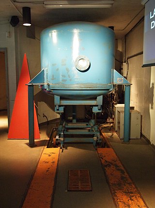
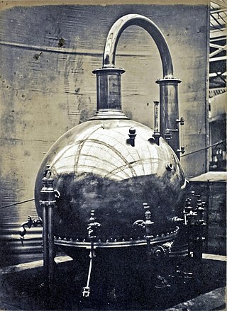
Vacuum deposition is a group of processes used to deposit layers of material atom-by-atom or molecule-by-molecule on a solid surface. These processes operate at pressures well below atmospheric pressure. The deposited layers can range from a thickness of one atom up to millimeters, forming freestanding structures. Multiple layers of different materials can be used, for example to form optical coatings. The process can be qualified based on the vapor source; physical vapor deposition uses a liquid or solid source and chemical vapor deposition uses a chemical vapor.

<span class="mw-page-title-main">Physical vapor deposition</span> Method of coating solid surfaces with thin films

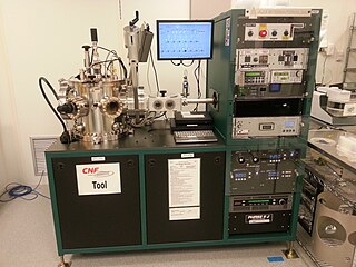
Physical vapor deposition (PVD), sometimes called physical vapor transport (PVT), describes a variety of vacuum deposition methods which can be used to produce thin films and coatings on substrates including metals, ceramics, glass, and polymers. PVD is characterized by a process in which the material transitions from a condensed phase to a vapor phase and then back to a thin film condensed phase. The most common PVD processes are sputtering and evaporation. PVD is used in the manufacturing of items which require thin films for optical, mechanical, electrical, acoustic or chemical functions. Examples include semiconductor devices such as thin-film solar cells, microelectromechanical devices such as thin film bulk acoustic resonator, aluminized PET film for food packaging and balloons, and titanium nitride coated cutting tools for metalworking. Besides PVD tools for fabrication, special smaller tools used mainly for scientific purposes have been developed.

<span class="mw-page-title-main">Thermal spraying</span> Coating process for applying heated materials to a surface

Thermal spraying techniques are coating processes in which melted materials are sprayed onto a surface. The "feedstock" is heated by electrical or chemical means.

Gas cluster ion beams (GCIB) is a technology for nano-scale modification of surfaces. It can smooth a wide variety of surface material types to within an angstrom of roughness without subsurface damage. It is also used to chemically alter surfaces through infusion or deposition.

<span class="mw-page-title-main">Plasma-enhanced chemical vapor deposition</span> Method of depositing thin films onto a substrate

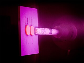
Plasma-enhanced chemical vapor deposition (PECVD) is a chemical vapor deposition process used to deposit thin films from a gas state (vapor) to a solid state on a substrate. Chemical reactions are involved in the process, which occur after creation of a plasma of the reacting gases. The plasma is generally created by radio frequency (RF) frequency or direct current (DC) discharge between two electrodes, the space between which is filled with the reacting gases.

<span class="mw-page-title-main">Evaporation (deposition)</span> Common method of thin-film deposition

Evaporation is a common method of thin-film deposition. The source material is evaporated in a vacuum. The vacuum allows vapor particles to travel directly to the target object (substrate), where they condense back to a solid state. Evaporation is used in microfabrication, and to make macro-scale products such as metallized plastic film.

<span class="mw-page-title-main">Sputter deposition</span> Method of thin film application

Sputter deposition is a physical vapor deposition (PVD) method of thin film deposition by the phenomenon of sputtering. This involves ejecting material from a "target" that is a source onto a "substrate" such as a silicon wafer. Resputtering is re-emission of the deposited material during the deposition process by ion or atom bombardment. Sputtered atoms ejected from the target have a wide energy distribution, typically up to tens of eV. The sputtered ions can ballistically fly from the target in straight lines and impact energetically on the substrates or vacuum chamber. Alternatively, at higher gas pressures, the ions collide with the gas atoms that act as a moderator and move diffusively, reaching the substrates or vacuum chamber wall and condensing after undergoing a random walk. The entire range from high-energy ballistic impact to low-energy thermalized motion is accessible by changing the background gas pressure. The sputtering gas is often an inert gas such as argon. For efficient momentum transfer, the atomic weight of the sputtering gas should be close to the atomic weight of the target, so for sputtering light elements neon is preferable, while for heavy elements krypton or xenon are used. Reactive gases can also be used to sputter compounds. The compound can be formed on the target surface, in-flight or on the substrate depending on the process parameters. The availability of many parameters that control sputter deposition make it a complex process, but also allow experts a large degree of control over the growth and microstructure of the film.

Ion beam mixing is the atomic intermixing and alloying that can occur at the interface separating two different materials during ion irradiation. It is applied as a process for adhering two multilayers, especially a substrate and deposited surface layer. The process involves bombarding layered samples with doses of ion radiation in order to promote mixing at the interface, and generally serves as a means of preparing electrical junctions, especially between non-equilibrium or metastable alloys and intermetallic compounds. Ion implantation equipment can be used to achieve ion beam mixing.

<span class="mw-page-title-main">Vapor–liquid–solid method</span> Mechanism to grow nano wires

The vapor–liquid–solid method (VLS) is a mechanism for the growth of one-dimensional structures, such as nanowires, from chemical vapor deposition. The growth of a crystal through direct adsorption of a gas phase on to a solid surface is generally very slow. The VLS mechanism circumvents this by introducing a catalytic liquid alloy phase which can rapidly adsorb a vapor to supersaturation levels, and from which crystal growth can subsequently occur from nucleated seeds at the liquid–solid interface. The physical characteristics of nanowires grown in this manner depend, in a controllable way, upon the size and physical properties of the liquid alloy.

<span class="mw-page-title-main">Neyco</span> French company

Neyco is a French company founded in 1954, specialist in High Vacuum, UHV, Inorganic materials and thin films.

References

  1. Harsha, K. S. S, "Principles of Physical Vapor Deposition of Thin Films", Elsevier, Great Britain (2006), p. 400.
  2. http://telemark.com/electron_beam_sources/arc_suppression.php?cat=1&id=Arc+Suppression+Sources. Archived 2012-12-12 at the Wayback Machine
  3. George, J., "Preparation of thin films", Marcel Dekker, Inc., New York (1992), p. 13–19.
  4. Madou, M. J., "Fundamentals of Microfabrication: The science of Miniaturization" 2nd Ed., CRC Press (2002), p. 135–6.
  5. Kesapragada, S. V.; Victor, P.; Nalamasu, O.; Gall, D. (2006). "Nanospring Pressure Sensors Grown by Glancing Angle Deposition". Nano Letters. American Chemical Society (ACS). 6 (4): 854–857. Bibcode:2006NanoL...6..854K. doi:10.1021/nl060122a. ISSN   1530-6984. PMID   16608297.
  6. Robbie, K.; Brett, M. J. (1997). "Sculptured thin films and glancing angle deposition: Growth mechanics and applications". Journal of Vacuum Science & Technology A: Vacuum, Surfaces, and Films. American Vacuum Society. 15 (3): 1460–1465. Bibcode:1997JVSTA..15.1460R. doi:10.1116/1.580562. ISSN   0734-2101.
  7. Driskell, Jeremy D.; Shanmukh, Saratchandra; Liu, Yongjun; Chaney, Stephen B.; Tang, X.-J.; Zhao, Y.-P.; Dluhy, Richard A. (2008). "The Use of Aligned Silver Nanorod Arrays Prepared by Oblique Angle Deposition as Surface Enhanced Raman Scattering Substrates". The Journal of Physical Chemistry C. American Chemical Society (ACS). 112 (4): 895–901. doi:10.1021/jp075288u. ISSN   1932-7447.

See also