3D microfabrication

Last updated

Three-dimensional (3D) microfabrication refers to manufacturing techniques that involve the layering of materials to produce a three-dimensional structure at a microscopic scale. [1] These structures are usually on the scale of micrometers and are popular in microelectronics and microelectromechanical systems.

Contents

Rapid prototyping

Much like their macroscopic analog, microstructures can be produced using rapid prototyping methods. These techniques generally involve the layering of some resin, with each layer being much thinner than that used for conventional processes in order to produce higher resolution microscopic components. Layers in processes such as electrochemical fabrication can be as thin as 5 to 10 μm. [2] The creation of microscopic structures is similar to conventional additive manufacturing techniques in that a computer aided design model is sliced into an appropriate number of two-dimensional layers in order to create a toolpath. This toolpath is then followed by a mechanical system to produce the desired geometry.

A popular application is stereolithography (SLA), which involves the use of a UV light or laser beam on a surface to create a layer, which are then lowered into a tank so that a new layer can be formed on top. Another commonly used method is fused deposition modeling (FDM), in which a moving head creates a layer by melting the model material (usually a polymer) and extrudes the melted material onto a surface. Other methods such as selective laser sintering (SLS) are also used in the additive manufacturing of 3D microstructures. [1]

3D laser microfabrication

Setup of a typical laser microfabrication 3D Laser Microfab.png
Setup of a typical laser microfabrication

Laser-based techniques are the most common approach for producing microstructures. Typical techniques involve the use of lasers to add or subtract material from a bulk sample. Recent applications of lasers involve the use of ultrashort pulses of lasers focused to a small area in order to create a pattern that is layered to create a structure. The use of lasers in such a manner is known as laser direct-writing (LDW). Microscopic mechanical elements such as micromotors, micropumps, and other microfluidic devices can be produced using direct-write concepts. In addition to additive and subtractive processes, LDW allows for the modification of the properties of a material. Mechanisms that allow for these modifications include sintering, microstereolithography, and multiphoton processes. These use a series of laser pulses to deliver a precise amount of energy to induce a physical or chemical change that can result in annealing and surface structuring of a material. [3]

Microstereolithography

Microstereolithography is a common technique based on stereolithography principles. 3D components are fabricated by repeatedly layering photopolymerizable resin and curing under an ultraviolet laser. Earlier systems that employ this technique use a scanning principle in which a focused light beam is fixed onto one location and the translation stage moves to fabricate each layer vector by vector. A faster alternate involves using a projection principle in which the image is projected onto the surface of the resin so that the irradiation of a layer is done in one step only. The high-resolution results allow for the fabrication of complex shapes that would otherwise be difficult to produce at such small scales. [1]

Multiphoton lithography

Multiphoton lithography, e.g., two-photon polymerization (2PP), can be used to 3D print structures with sub-micrometer resolution. The process uses the focal point of a laser to photopolymerize the resin or glass at a specific point. In 2PP, two photons meet at the focal point, doubling the laser's frequency and curing a voxel of 2PP resin while having a minimum effect on the material around the voxel/focal point. By moving the focal point around in three-dimensional space and solidifying the medium at different points, the desired 3D geometry can be additively manufactured with feature size down to 100-160 nm as of 2023. [4] The limits of 2PP fabrication depend on the utilized equipment (servo, mirrors, and laser resolution) and selected lens (laser focusing), as well as the material (UV absorption profile and reactivity). [3] Recently, a list of 2PP printed materials has been actively expanding and includes hard and flexible polymers, glass, soft elastomers, enabling microfabrication of various MEMS and soft microbotics. [5]

Other additive processes

Additive processes involve the layering of materials in a certain pattern. These include laser chemical vapor deposition (LCVD), which use organic precursors to write patterns on a structure or bulk material. This application can be found in the field of electronics, particularly in the repair of transistor arrays for displays. Another additive process is laser-induced forward transfer (LIFT), which uses pulsed lasers aimed at a coated substrate to transfer material in the direction of the laser flow. [1] LIFT has been used to produce transfer thermo-electric materials, polymers [6] and has been used to print copper wires. [7]

With inclined/rotated UV lithography

Focus on the 3D microstructures now, it have been focused in a lot of microsystems like electronic, mechanical, micro-optical and analysis systems. And when this technology is developing, we found that the traditional and conventional micro machining technologies like surface micromachining, bulk micromachining and GIGA process are not sufficient to fabricate or produce oblique and curved 3D microstructures. [8]

Fabrication

The basic setup of inclined UV exposure has conventional UV source, a contact stage, and a tilting stage. Plus, we place a photomask and a photoresist coated substrate between the upper and lower plates of the contact stage, and it is fixed by pushing up the lower plate with a screw. Then, we can expose the photoresist to the inclined UV.

An example of the fabrication process: Su-8 is a negative thick photoresist, which used in novel 3D micro fabrication method with inclined/rotated UV lithography. During the process, we coat SU-8 50 on a silicon wafer with a thickness of about 100ųm. Then, soft bake the resist on a 65 °C hot plate for 10 minutes and on a 95 °C plate for 30 minutes. It is contacted with a photomask using the contact stage. This stage, is leaned against the tilting stage and the resist is exposed to the UV. The dose of 365 nm UV is 500mJ/cm2. After the exposure, the resist is post-exposure baked on a 65 °C hot plate for 3 minutes and on a 95 °C plate for 10 minutes. In the end, the resist is developed in the SU-8 for about 10 to 15 minutes at the room temperature with mild agitation and then, rinsed with isopropyl alcohol. Besides that, there can be a lot of other procedures. For example, inclined UV lithography, inclined and rotated UV lithography and lithography using reflected UV.

When the trace of the incident UV with a right angle is on a straight line, so the patterns of a photomask are transcribed to the resist. When talking about inclined UV exposure processes, the UV is refracted and reflected, this makes it possible to fabricate various of 3D structures. The microstructures fabricated by the 3D micro fabrication technology can be allied to a lot of microsystems directly. Also, it can be used as the molds for electroplating. As a result, these technology can be applied to a variety of fields like filters, mixers, jets, micro channels, light guide panels of LCD monitor and more.

Self-folding materials

Design of complicated 3D microstructure can be highly challenging task for development of novel materials for optics, biotechnology and micro/nano electronics. 3D materials can be fabricated using a lot of methods like two-photon photolithography, interference lithography and molding. But 3D structuring using these techniques is very complicated, experimentally. This can limit their upscaling and broad applicability.

Nature offers a large number of ideas for the design of novel materials with superior properties. Self-assembly and self-organization being the main principle of structure formation in nature attract significant interest as promising concepts for the design of intelligent materials.

Stimuli-responsive hydrogels mimic swelling/shrinking behavior of plant cells and produce macroscopic actuation in response to a small variation of environmental conditions. Mostly, homogenous expansion or contraction in all directions can result a change of conditions. Also, inhomogeneous expansion and shrinkage can result more complex behavior like bending, twisting and folding and they can happen with different magnitudes in different directions. Utilization of these phenomena for the design of structured materials can be highly attractive because they allow simple, template-free fabrication of very complex repetitive 2D and 3D patterns. However, they cannot be prepared by using sophisticated fabrication methods like two-photon and interference photolithography as mentioned before. There is an advantage of the self-folding approach, is the possibility of quick, reversible, and reproducible fabrication of 3D hollow objects with controlled chemical properties and morphology of both the exterior and the interior.

One experimental application of self-folding materials is pasta that ships flat but folds into the desired shape on contact with boiling water. [9]

Outlook

One factor that limit broad applicability of self-folding polymer films is the manufacturing cost. Actually, polymer can be deposited by spinning and dipping coating at ambient conditions, the fabrication of polymer self-folding films is substantially cheaper than fabrication of inorganic ones, which are produced by vacuum deposition. In another word, there is no method, which is cheap and large-scale production of self-folding polymer films that substantially limits their application.

To solve these issues, the future research must be focused on deeper investigation of folding to allow design of complex 3D structures using just 2D shapes. On the other hand, searching a way, which is cheap and fast manufacturing of large quantity of self-folding films can be greatly helpful. [10]

Related Research Articles

Photolithography is a process used in the manufacturing of integrated circuits. It involves using light to transfer a pattern onto a substrate, typically a silicon wafer.

<span class="mw-page-title-main">Photoresist</span> Light-sensitive material used in making electronics

A photoresist is a light-sensitive material used in several processes, such as photolithography and photoengraving, to form a patterned coating on a surface. This process is crucial in the electronics industry.

<span class="mw-page-title-main">Selective laser sintering</span> 3D printing technique

Selective laser sintering (SLS) is an additive manufacturing (AM) technique that uses a laser as the power and heat source to sinter powdered material, aiming the laser automatically at points in space defined by a 3D model, binding the material together to create a solid structure. It is similar to selective laser melting; the two are instantiations of the same concept but differ in technical details. SLS is a relatively new technology that so far has mainly been used for rapid prototyping and for low-volume production of component parts. Production roles are expanding as the commercialization of AM technology improves.

<span class="mw-page-title-main">Stereolithography</span> 3D printing technique

Stereolithography is a form of 3D printing technology used for creating models, prototypes, patterns, and production parts in a layer by layer fashion using photochemical processes by which light causes chemical monomers and oligomers to cross-link together to form polymers. Those polymers then make up the body of a three-dimensional solid. Research in the area had been conducted during the 1970s, but the term was coined by Chuck Hull in 1984 when he applied for a patent on the process, which was granted in 1986. Stereolithography can be used to create prototypes for products in development, medical models, and computer hardware, as well as in many other applications. While stereolithography is fast and can produce almost any design, it can be expensive.

<span class="mw-page-title-main">3D printing</span> Additive process used to make a three-dimensional object

3D printing or additive manufacturing is the construction of a three-dimensional object from a CAD model or a digital 3D model. It can be done in a variety of processes in which material is deposited, joined or solidified under computer control, with the material being added together, typically layer by layer.

Nanolithography (NL) is a growing field of techniques within nanotechnology dealing with the engineering of nanometer-scale structures on various materials.

In semiconductor fabrication, a resist is a thin layer used to transfer a circuit pattern to the semiconductor substrate which it is deposited upon. A resist can be patterned via lithography to form a (sub)micrometer-scale, temporary mask that protects selected areas of the underlying substrate during subsequent processing steps. The material used to prepare said thin layer is typically a viscous solution. Resists are generally proprietary mixtures of a polymer or its precursor and other small molecules that have been specially formulated for a given lithography technology. Resists used during photolithography are called photoresists.

<span class="mw-page-title-main">Nanoimprint lithography</span> Method of fabricating nanometer scale patterns using a special stamp

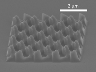
Nanoimprint lithography (NIL) is a method of fabricating nanometer-scale patterns. It is a simple nanolithography process with low cost, high throughput and high resolution. It creates patterns by mechanical deformation of imprint resist and subsequent processes. The imprint resist is typically a monomer or polymer formulation that is cured by heat or UV light during the imprinting. Adhesion between the resist and the template is controlled to allow proper release.

<span class="mw-page-title-main">Microfabrication</span> Fabrication at micrometre scales and smaller

Microfabrication is the process of fabricating miniature structures of micrometre scales and smaller. Historically, the earliest microfabrication processes were used for integrated circuit fabrication, also known as "semiconductor manufacturing" or "semiconductor device fabrication". In the last two decades microelectromechanical systems (MEMS), microsystems, micromachines and their subfields, microfluidics/lab-on-a-chip, optical MEMS, RF MEMS, PowerMEMS, BioMEMS and their extension into nanoscale have re-used, adapted or extended microfabrication methods. Flat-panel displays and solar cells are also using similar techniques.

<span class="mw-page-title-main">SU-8 photoresist</span> Epoxy-based polymer

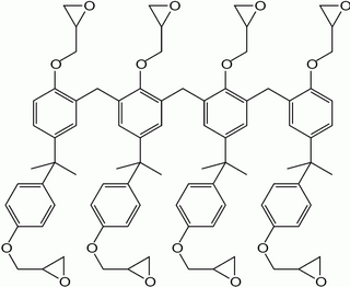
SU-8 is a commonly used epoxy-based negative photoresist. Negative refers to a photoresist whereby the parts exposed to UV become cross-linked, while the remainder of the film remains soluble and can be washed away during development.

<span class="mw-page-title-main">LIGA</span> Fabrication technology used to create high-aspect-ratio microstructures

LIGA is a fabrication technology used to create high-aspect-ratio microstructures. The term is a German acronym for Lithographie, Galvanoformung, Abformung – lithography, electroplating, and molding.

Interference lithography is a technique for patterning regular arrays of fine features, without the use of complex optical systems or photomasks.

<span class="mw-page-title-main">Rapid prototyping</span> Group of techniques to quickly construct physical objects

Rapid prototyping is a group of techniques used to quickly fabricate a scale model of a physical part or assembly using three-dimensional computer aided design (CAD) data. Construction of the part or assembly is usually done using 3D printing or "additive layer manufacturing" technology.

Digital modeling and fabrication is a design and production process that combines 3D modeling or computing-aided design (CAD) with additive and subtractive manufacturing. Additive manufacturing is also known as 3D printing, while subtractive manufacturing may also be referred to as machining, and many other technologies can be exploited to physically produce the designed objects.

<span class="mw-page-title-main">Multiphoton lithography</span> Technique for creating microscopic structures

Multiphoton lithography of polymer templates has been known for years by the photonic crystal community. Similar to standard photolithography techniques, structuring is accomplished by illuminating negative-tone or positive-tone photoresists via light of a well-defined wavelength. A critical difference is, however, the avoidance of photomasks. Instead, two-photon absorption is utilized to induce a dramatic change in the solubility of the resist for appropriate developers.

Projection micro-stereolithography (PµSL) adapts 3D printing technology for micro-fabrication. Digital micro display technology provides dynamic stereolithography masks that work as a virtual photomask. This technique allows for rapid photopolymerization of an entire layer with a flash of UV illumination at micro-scale resolution. The mask can control individual pixel light intensity, allowing control of material properties of the fabricated structure with desired spatial distribution.

<span class="mw-page-title-main">Foturan</span>

Foturan is a photosensitive glass by SCHOTT Corporation developed in 1984. It is a technical glass-ceramic which can be structured without photoresist when it is exposed to shortwave radiation such as ultraviolet light and subsequently etched.

<span class="mw-page-title-main">3D printing processes</span> List of 3D printing processes

A variety of processes, equipment, and materials are used in the production of a three-dimensional object via additive manufacturing. 3D printing is also known as additive manufacturing, because the numerous available 3D printing process tend to be additive in nature, with a few key differences in the technologies and the materials used in this process.

Microscale structural metamaterials are synthetic structures that are aimed to yield specific desired mechanical advantages. These designs are often inspired by natural cellular materials such as plant and bone tissue which have superior mechanical efficiency due to their low weight to stiffness ratios.

Multi-material 3D printing is the additive manufacturing procedure of using multiple materials at the same time to fabricate an object. Similar to single material additive manufacturing it can be realised through methods such as FFF, SLA and Inkjet 3D printing. By expanding the design space to different materials, it establishes the possibilities of creating 3D printed objects of different color or with different material properties like elasticity or solubility. The first multi-material 3D printer Fab@Home became publicly available in 2006. The concept was quickly adopted by the industry followed by many consumer ready multi-material 3D printers.

References

  1. 1 2 3 4 Baldacchini, Tommasso, ed. (2016). Three-Dimensional Microfabrication Using Two-Photon Polymerization: Fundamentals, Technology, and Applications. Elsevier. ISBN   978-0-323-35321-2.
  2. Groover, Mikell (2012). Fundamentals of Modern Manufacturing: Materials, Processes, and Systems (5 ed.). Wiley. p. 846. ISBN   978-1118231463.
  3. 1 2 Misawa, Hiroaki, ed. (2006). 3D Laser Microfabrication: Principles and Applications. Germany: Wiley. ISBN   978-3-527-31055-5.
  4. "Photonic Professional GT2". Nanoscribe. Retrieved 25 November 2023.
  5. Srinivasaraghavan Govindarajan, Rishikesh; Sikulskyi, Stanislav; Ren, Zefu; Stark, Taylor; Kim, Daewon (10 November 2023). "Characterization of Photocurable IP-PDMS for Soft Micro Systems Fabricated by Two-Photon Polymerization 3D Printing". Polymers. 15 (22): 4377. doi: 10.3390/polym15224377 . PMC   10675433 . PMID   38006101.
  6. Heath, Daniel J; Feinaeugle, Matthias; Grant-Jacob, James A; Mills, Ben; Eason, Robert W (2015-05-01). "Dynamic spatial pulse shaping via a digital micromirror device for patterned laser-induced forward transfer of solid polymer films". Optical Materials Express. 5 (5): 1129. Bibcode:2015OMExp...5.1129H. doi: 10.1364/OME.5.001129 . ISSN   2159-3930.
  7. Grant-Jacob, James A.; Mills, Benjamin; Feinaeugle, Matthias; Sones, Collin L.; Oosterhuis, Gerrit; Hoppenbrouwers, Marc B.; Eason, Robert W. (2013-06-01). "Micron-scale copper wires printed using femtosecond laser-induced forward transfer with automated donor replenishment". Optical Materials Express. 3 (6): 747–754. Bibcode:2013OMExp...3..747G. doi: 10.1364/OME.3.000747 . ISSN   2159-3930.
  8. Han, Manhee (2004). Sensors and Actuators A: Physical.
  9. Nanos, Janelle (June 5, 2017), "MIT researchers develop a shape-shifting pasta", The Boston Globe
  10. Ionov, Leonid (2013). Polymer Reviews, 2013, Vol.53(1). Germany: Taylor & Francis Group. pp. 92–107.