Related Research Articles

Chemical vapor deposition (CVD) is a vacuum deposition method used to produce high-quality, and high-performance, solid materials. The process is often used in the semiconductor industry to produce thin films.

A transistor is a semiconductor device used to amplify or switch electrical signals and power. It is one of the basic building blocks of modern electronics. It is composed of semiconductor material, usually with at least three terminals for connection to an electronic circuit. A voltage or current applied to one pair of the transistor's terminals controls the current through another pair of terminals. Because the controlled (output) power can be higher than the controlling (input) power, a transistor can amplify a signal. Some transistors are packaged individually, but many more in miniature form are found embedded in integrated circuits. Because transistors are the key active components in practically all modern electronics, many people consider them one of the 20th century's greatest inventions.
SiGe, or silicon–germanium, is an alloy with any molar ratio of silicon and germanium, i.e. with a molecular formula of the form Si1−xGex. It is commonly used as a semiconductor material in integrated circuits (ICs) for heterojunction bipolar transistors or as a strain-inducing layer for CMOS transistors. IBM introduced the technology into mainstream manufacturing in 1989. This relatively new technology offers opportunities in mixed-signal circuit and analog circuit IC design and manufacture. SiGe is also used as a thermoelectric material for high-temperature applications (>700 K).
In solid-state physics, the electron mobility characterises how quickly an electron can move through a metal or semiconductor when pulled by an electric field. There is an analogous quantity for holes, called hole mobility. The term carrier mobility refers in general to both electron and hole mobility.

A high-electron-mobility transistor, also known as heterostructure FET (HFET) or modulation-doped FET (MODFET), is a field-effect transistor incorporating a junction between two materials with different band gaps as the channel instead of a doped region. A commonly used material combination is GaAs with AlGaAs, though there is wide variation, dependent on the application of the device. Devices incorporating more indium generally show better high-frequency performance, while in recent years, gallium nitride HEMTs have attracted attention due to their high-power performance. Like other FETs, HEMTs are used in integrated circuits as digital on-off switches. FETs can also be used as amplifiers for large amounts of current using a small voltage as a control signal. Both of these uses are made possible by the FET’s unique current–voltage characteristics. HEMT transistors are able to operate at higher frequencies than ordinary transistors, up to millimeter wave frequencies, and are used in high-frequency products such as cell phones, satellite television receivers, voltage converters, and radar equipment. They are widely used in satellite receivers, in low power amplifiers and in the defense industry.
In semiconductor production, doping is the intentional introduction of impurities into an intrinsic semiconductor for the purpose of modulating its electrical, optical and structural properties. The doped material is referred to as an extrinsic semiconductor.
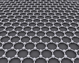
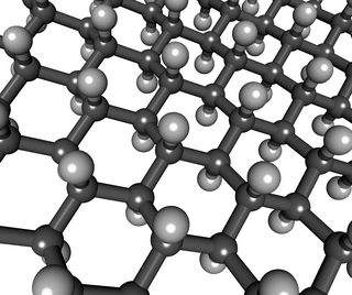
Graphene is an allotrope of carbon consisting of a single layer of atoms arranged in a hexagonal lattice nanostructure. The name is derived from "graphite" and the suffix -ene, reflecting the fact that the graphite allotrope of carbon contains numerous double bonds.

Strained silicon is a layer of silicon in which the silicon atoms are stretched beyond their normal interatomic distance. This can be accomplished by putting the layer of silicon over a substrate of silicon–germanium. As the atoms in the silicon layer align with the atoms of the underlying silicon germanium layer, the links between the silicon atoms become stretched - thereby leading to strained silicon. Moving these silicon atoms farther apart reduces the atomic forces that interfere with the movement of electrons through the transistors and thus better mobility, resulting in better chip performance and lower energy consumption. These electrons can move 70% faster allowing strained silicon transistors to switch 35% faster.

Phosphorene is a two-dimensional material consisting of phosphorus. It consists of a single layer of black phosphorus, the most stable allotrope of phosphorus. Phosphorene is analogous to graphene. Among two-dimensional materials, phosphorene is a competitor to graphene because it has a nonzero fundamental band gap that can be modulated by strain and the number of layers in a stack. Phosphorene was first isolated in 2014 by mechanical exfoliation. Liquid exfoliation is a promising method for scalable phosphorene production.
Graphane is a two-dimensional polymer of carbon and hydrogen with the formula unit (CH)n where n is large. Partial hydrogenation results in hydrogenated graphene, which was reported by Elias et al in 2009 by a TEM study to be "direct evidence for a new graphene-based derivative". The authors viewed the panorama as "a whole range of new two-dimensional crystals with designed electronic and other properties".
Silicene is a two-dimensional allotrope of silicon, with a hexagonal honeycomb structure similar to that of graphene. Contrary to graphene, silicene is not flat, but has a periodically buckled topology; the coupling between layers in silicene is much stronger than in multilayered graphene; and the oxidized form of silicene, 2D silica, has a very different chemical structure from graphene oxide.
Bilayer graphene is a material consisting of two layers of graphene. One of the first reports of bilayer graphene was in the seminal 2004 Science paper by Geim and colleagues, in which they described devices "which contained just one, two, or three atomic layers"

The field-effect transistor (FET) is a type of transistor that uses an electric field to control the flow of current in a semiconductor. It comes in two types: junction-gate FET (JFET) and metal-oxide-semiconductor FET (MOSFET). FETs have three terminals: source, gate, and drain. FETs control the flow of current by the application of a voltage to the gate, which in turn alters the conductivity between the drain and source.
Potential graphene applications include lightweight, thin, and flexible electric/photonics circuits, solar cells, and various medical, chemical and industrial processes enhanced or enabled by the use of new graphene materials.

Transition-metal dichalcogenide (TMD or TMDC) monolayers are atomically thin semiconductors of the type MX2, with M a transition-metal atom (Mo, W, etc.) and X a chalcogen atom (S, Se, or Te). One layer of M atoms is sandwiched between two layers of X atoms. They are part of the large family of so-called 2D materials, named so to emphasize their extraordinary thinness. For example, a MoS2 monolayer is only 6.5 Å thick. The key feature of these materials is the interaction of large atoms in the 2D structure as compared with first-row transition-metal dichalcogenides, e.g., WTe2 exhibits anomalous giant magnetoresistance and superconductivity.
In materials science, the term single-layer materials or 2D materials refers to crystalline solids consisting of a single layer of atoms. These materials are promising for some applications but remain the focus of research. Single-layer materials derived from single elements generally carry the -ene suffix in their names, e.g. graphene. Single-layer materials that are compounds of two or more elements have -ane or -ide suffixes. 2D materials can generally be categorized as either 2D allotropes of various elements or as compounds.

Germanene is a material made up of a single layer of germanium atoms. The material is created in a process similar to that of silicene and graphene, in which high vacuum and high temperature are used to deposit a layer of germanium atoms on a substrate. High-quality thin films of germanene have revealed unusual two-dimensional structures with novel electronic properties suitable for semiconductor device applications and materials science research.
A two-dimensional semiconductor is a type of natural semiconductor with thicknesses on the atomic scale. Geim and Novoselov et al. initiated the field in 2004 when they reported a new semiconducting material graphene, a flat monolayer of carbon atoms arranged in a 2D honeycomb lattice. A 2D monolayer semiconductor is significant because it exhibits stronger piezoelectric coupling than traditionally employed bulk forms. This coupling could enable applications. One research focus is on designing nanoelectronic components by the use of graphene as electrical conductor, hexagonal boron nitride as electrical insulator, and a transition metal dichalcogenide as semiconductor.
A rapidly increasing list of graphene production techniques have been developed to enable graphene's use in commercial applications.
Graphene is the only form of carbon in which every atom is available for chemical reaction from two sides. Atoms at the edges of a graphene sheet have special chemical reactivity. Graphene has the highest ratio of edge atoms of any allotrope. Defects within a sheet increase its chemical reactivity. The onset temperature of reaction between the basal plane of single-layer graphene and oxygen gas is below 260 °C (530 K). Graphene combusts at 350 °C (620 K). Graphene is commonly modified with oxygen- and nitrogen-containing functional groups and analyzed by infrared spectroscopy and X-ray photoelectron spectroscopy. However, determination of structures of graphene with oxygen- and nitrogen- functional groups requires the structures to be well controlled.
References
- ↑ Garcia, J. C.; de Lima, D. B.; Assali, L. V. C.; Justo, J. F. (2011). "Group IV Graphene- and Graphane-Like Nanosheets". J. Phys. Chem. C. 115: 13242. arXiv: 1204.2875 . doi:10.1021/jp203657w.
- 1 2 "'Germanane' may replace silicon for lighter, faster electronics". KurzweilAI. Retrieved 2013-04-12.
- ↑ Amamou, W.; Odenthal, P. M.; Bushong, E. J.; O'Hara, D. J.; Luo, Y. K.; van Baren, J.; Pinchuk, I.; Wu, Y.; Ahmed, A. S.; Katoch, J.; Bockrath, M. W.; Tom, H. W. K.; Goldberger, J. E.; Kawakami, R. K. (2015). "Large area epitaxial germanane for electronic devices". 2D Materials. 2 (3): 035012. Bibcode:2015TDM.....2c5012A. doi: 10.1088/2053-1583/2/3/035012 .
- ↑ Madhushankar, B. N.; Kaverzin, A.; Giousis, T.; Potsi, G.; Gournis, D.; Rudolf, P.; Blake, G. R.; Van Der Wal, C. H.; Van Wees, B. J. (2017). "Electronic properties of germanane field-effect transistors". 2D Materials. 4 (2): 021009. Bibcode:2017TDM.....4b1009M. doi: 10.1088/2053-1583/aa57fd .
- ↑ "Flash Nano: Germanane FET shows real promise for optoelectronics - nanotechweb.org". Archived from the original on 2017-02-18. Retrieved 2017-02-17.