The aspect ratio of a geometric shape is the ratio of its sizes in different dimensions. For example, the aspect ratio of a rectangle is the ratio of its longer side to its shorter side—the ratio of width to height, when the rectangle is oriented as a "landscape".
Liga or LIGA may refer to:
Micro process engineering is the science of conducting chemical or physical processes inside small volumina, typically inside channels with diameters of less than 1 mm (microchannels) or other structures with sub-millimeter dimensions. These processes are usually carried out in continuous flow mode, as opposed to batch production, allowing a throughput high enough to make micro process engineering a tool for chemical production. Micro process engineering is therefore not to be confused with microchemistry, which deals with very small overall quantities of matter.

Microstructure is the very small scale structure of a material, defined as the structure of a prepared surface of material as revealed by an optical microscope above 25× magnification. The microstructure of a material can strongly influence physical properties such as strength, toughness, ductility, hardness, corrosion resistance, high/low temperature behaviour or wear resistance. These properties in turn govern the application of these materials in industrial practice.

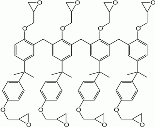
SU-8 is a commonly used epoxy-based negative photoresist. Negative refers to a photoresist whereby the parts exposed to UV become cross-linked, while the remainder of the film remains soluble and can be washed away during development.

LIGA is a fabrication technology used to create high-aspect-ratio microstructures. The term is a German acronym for Lithographie, Galvanoformung, Abformung – lithography, electroplating, and molding.

Etching is used in microfabrication to chemically remove layers from the surface of a wafer during manufacturing. Etching is a critically important process module in fabrication, and every wafer undergoes many etching steps before it is complete.
Electron-beam additive manufacturing, or electron-beam melting (EBM) is a type of additive manufacturing, or 3D printing, for metal parts. The raw material is placed under a vacuum and fused together from heating by an electron beam. This technique is distinct from selective laser sintering as the raw material fuses have completely melted. Selective Electron Beam Melting (SEBM) emerged as a powder bed-based additive manufacturing (AM) technology and was brought to market in 1997 by Arcam AB Corporation headquartered in Sweden.
Acicular ferrite is a microstructure of ferrite in steel that is characterised by needle-shaped crystallites or grains when viewed in two dimensions. The grains, actually three-dimensional in shape, have a thin lenticular shape. This microstructure is advantageous over other microstructures for steel because of its chaotic ordering, which increases toughness.
The Max Planck Institute of Microstructure Physics in Halle (Saale) is a research institute in Germany focused novel materials with useful functionalities. Active research topics includes spintronics, neuromorphic systems, nano-photonics, topological metals and insulators etc. It was founded in 1992 by Hellmut Fischmeister and is a follow-up to the German Academy of Sciences Institute of Solid State Physics and Electron Microscopy. The institute moved into new buildings from 1997 till 1999. It is one of 84 institutes in the Max Planck Society (Max-Planck-Gesellschaft).

Dual-phase steel (DP steel) is a high-strength steel that has a ferritic–martensitic microstructure. DP steels are produced from low or medium carbon steels that are quenched from a temperature above A1 but below A3 determined from continuous cooling transformation diagram. This results in a microstructure consisting of a soft ferrite matrix containing islands of martensite as the secondary phase (martensite increases the tensile strength). Therefore, the overall behaviour of DP steels is governed by the volume fraction, morphology (size, aspect ratio, interconnectivity, etc.), the grain size and the carbon content. For achieving these microstructures, DP steels typically contain 0.06–0.15 wt.% C and 1.5-3% Mn (the former strengthens the martensite, and the latter causes solid solution strengthening in ferrite, while both stabilize the austenite), Cr & Mo (to retard pearlite or bainite formation), Si (to promote ferrite transformation), V and Nb (for precipitation strengthening and microstructure refinement). The desire to produce high strength steels with formability greater than microalloyed steel led to development of DP steels in 2007 by Tata Steel.
Micromachining may refer to:
Superconductor Science and Technology is a peer-reviewed scientific journal covering research on all aspects of superconductivity, including theories on superconductivity, the basic physics of superconductors, the relation of microstructure and growth to superconducting properties, the theory of novel devices, and the fabrication and properties of thin films and devices. The editor-in-chief is Cathy P Foley (CSIRO). It was established in 1988 and it is published by IOP Publishing. According to the Journal Citation Reports, the journal has an impact factor of 3.7 for 2023.

Foturan is a photosensitive glass by SCHOTT Corporation developed in 1984. It is a technical glass-ceramic which can be structured without photoresist when it is exposed to shortwave radiation such as ultraviolet light and subsequently etched.
Three-dimensional (3D) microfabrication refers to manufacturing techniques that involve the layering of materials to produce a three-dimensional structure at a microscopic scale. These structures are usually on the scale of micrometers and are popular in microelectronics and microelectromechanical systems.

Silicon nanowires, also referred to as SiNWs, are a type of semiconductor nanowire most often formed from a silicon precursor by etching of a solid or through catalyzed growth from a vapor or liquid phase. Such nanowires have promising applications in lithium-ion batteries, thermoelectrics and sensors. Initial synthesis of SiNWs is often accompanied by thermal oxidation steps to yield structures of accurately tailored size and morphology.
Friction extrusion is a thermo-mechanical process that can be used to form fully consolidated wire, rods, tubes, or other non-circular metal shapes directly from a variety of precursor charges including metal powder, flake, machining waste or solid billet. The process imparts unique, and potentially, highly desirable microstructures to the resulting products. Friction extrusion was invented at The Welding Institute in the UK and patented in 1991. It was originally intended primarily as a method for production of homogeneous microstructures and particle distributions in metal matrix composite materials.
In integrated circuits (ICs), interconnects are structures that connect two or more circuit elements together electrically. The design and layout of interconnects on an IC is vital to its proper function, performance, power efficiency, reliability, and fabrication yield. The material interconnects are made from depends on many factors. Chemical and mechanical compatibility with the semiconductor substrate and the dielectric between the levels of interconnect is necessary, otherwise barrier layers are needed. Suitability for fabrication is also required; some chemistries and processes prevent the integration of materials and unit processes into a larger technology (recipe) for IC fabrication. In fabrication, interconnects are formed during the back-end-of-line after the fabrication of the transistors on the substrate.

Adriana Eleni Lita is a Romanian materials scientist who is a member of the faint photonics group at National Institute of Standards and Technology. She works on fabrication and development of single-photon detectors such as transition-edge sensors and superconducting nanowire single-photon detector devices.

The use of microstructures in 3D printing, where the thickness of each strut scale of tens of microns ranges from 0.2mm to 0.5mm, has the capabilities necessary to change the physical properties of objects (metamaterials) such as: elasticity, resistance, and hardness. In other words, these capabilities allow physical objects to become lighter or more flexible. The pattern has to adhere to geometric constraints, and thickness constraints, or can be enforced using optimization methods. Innovations in this field are being discovered in addition to 3D printers being built and researched with the intent to specialize in building structures needing altered physical properties.


