Related Research Articles

A crystal or crystalline solid is a solid material whose constituents are arranged in a highly ordered microscopic structure, forming a crystal lattice that extends in all directions. In addition, macroscopic single crystals are usually identifiable by their geometrical shape, consisting of flat faces with specific, characteristic orientations. The scientific study of crystals and crystal formation is known as crystallography. The process of crystal formation via mechanisms of crystal growth is called crystallization or solidification.

Chemical vapor deposition (CVD) is a vacuum deposition method used to produce high quality, high-performance, solid materials. The process is often used in the semiconductor industry to produce thin films.

The interdisciplinary field of materials science, also commonly termed materials science and engineering, covers the design and discovery of new materials, particularly solids. The intellectual origins of materials science stem from the Enlightenment, when researchers began to use analytical thinking from chemistry, physics, and engineering to understand ancient, phenomenological observations in metallurgy and mineralogy. Materials science still incorporates elements of physics, chemistry, and engineering. As such, the field was long considered by academic institutions as a sub-field of these related fields. Beginning in the 1940s, materials science began to be more widely recognized as a specific and distinct field of science and engineering, and major technical universities around the world created dedicated schools for its study.

Sintering or frittage is the process of compacting and forming a solid mass of material by heat or pressure without melting it to the point of liquefaction.

Silicon carbide (SiC), also known as carborundum, is a semiconductor containing silicon and carbon. It occurs in nature as the extremely rare mineral moissanite. Synthetic SiC powder has been mass-produced since 1893 for use as an abrasive. Grains of silicon carbide can be bonded together by sintering to form very hard ceramics that are widely used in applications requiring high endurance, such as car brakes, car clutches and ceramic plates in bulletproof vests. Electronic applications of silicon carbide such as light-emitting diodes (LEDs) and detectors in early radios were first demonstrated around 1907. SiC is used in semiconductor electronics devices that operate at high temperatures or high voltages, or both. Large single crystals of silicon carbide can be grown by the Lely method and they can be cut into gems known as synthetic moissanite.

An ingot is a piece of relatively pure material, usually metal, that is cast into a shape suitable for further processing. In steelmaking, it is the first step among semi-finished casting products. Ingots usually require a second procedure of shaping, such as cold/hot working, cutting, or milling to produce a useful final product. Non-metallic and semiconductor materials prepared in bulk form may also be referred to as ingots, particularly when cast by mold based methods. Precious metal ingots can be used as currency, or as a currency reserve, as with gold bars.

A crystallite is a small or even microscopic crystal which forms, for example, during the cooling of many materials. Crystallites are also referred to as grains.

Epitaxy refers to a type of crystal growth or material deposition in which new crystalline layers are formed with one or more well-defined orientations with respect to the crystalline substrate. The deposited crystalline film is called an epitaxial film or epitaxial layer. The relative orientation(s) of the epitaxial layer to the crystalline substrate is defined in terms of the orientation of the crystal lattice of each material. For epitaxial growth, the new layer must be crystalline and each crystallographic domain of the overlayer must have a well-defined orientation relative to the substrate crystal structure. Amorphous growth or multicrystalline growth with random crystal orientation does not meet this criterion. For most technological applications, single domain epitaxy, which is the growth of an overlayer crystal with one well-defined orientation with respect to the substrate crystal, is preferred.
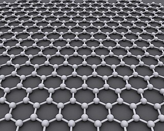
Graphene is an allotrope of carbon consisting of a single layer of atoms arranged in a two-dimensional honeycomb lattice. The name is a portmanteau of "graphite" and the suffix -ene, reflecting the fact that the graphite allotrope of carbon consists of stacked graphene layers.
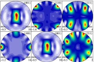
In materials science, texture is the distribution of crystallographic orientations of a polycrystalline sample. A sample in which these orientations are fully random is said to have no distinct texture. If the crystallographic orientations are not random, but have some preferred orientation, then the sample has a weak, moderate or strong texture. The degree is dependent on the percentage of crystals having the preferred orientation. Texture is seen in almost all engineered materials, and can have a great influence on materials properties. Also, geologic rocks show texture due to their thermo-mechanic history of formation processes.
In materials science, the sol–gel process is a method for producing solid materials from small molecules. The method is used for the fabrication of metal oxides, especially the oxides of silicon (Si) and titanium (Ti). The process involves conversion of monomers into a colloidal solution (sol) that acts as the precursor for an integrated network of either discrete particles or network polymers. Typical precursors are metal alkoxides.
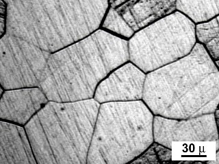
A grain boundary is the interface between two grains, or crystallites, in a polycrystalline material. Grain boundaries are 2D defects in the crystal structure, and tend to decrease the electrical and thermal conductivity of the material. Most grain boundaries are preferred sites for the onset of corrosion and for the precipitation of new phases from the solid. They are also important to many of the mechanisms of creep. On the other hand, grain boundaries disrupt the motion of dislocations through a material, so reducing crystallite size is a common way to improve mechanical strength, as described by the Hall–Petch relationship. The study of grain boundaries and their effects on the mechanical, electrical and other properties of materials forms an important topic in materials science.
A single-crystal, or monocrystalline, solid is a material in which the crystal lattice of the entire sample is continuous and unbroken to the edges of the sample, with no grain boundaries. The absence of the defects associated with grain boundaries can give monocrystals unique properties, particularly mechanical, optical and electrical, which can also be anisotropic, depending on the type of crystallographic structure. These properties, in addition to making them precious in some gems, are industrially used in technological applications, especially in optics and electronics.

The vapor–liquid–solid method (VLS) is a mechanism for the growth of one-dimensional structures, such as nanowires, from chemical vapor deposition. The growth of a crystal through direct adsorption of a gas phase on to a solid surface is generally very slow. The VLS mechanism circumvents this by introducing a catalytic liquid alloy phase which can rapidly adsorb a vapor to supersaturation levels, and from which crystal growth can subsequently occur from nucleated seeds at the liquid–solid interface. The physical characteristics of nanowires grown in this manner depend, in a controllable way, upon the size and physical properties of the liquid alloy.

Graphite oxide, formerly called graphitic oxide or graphitic acid, is a compound of carbon, oxygen, and hydrogen in variable ratios, obtained by treating graphite with strong oxidizers and acids for resolving of extra metals. The maximally oxidized bulk product is a yellow solid with C:O ratio between 2.1 and 2.9, that retains the layer structure of graphite but with a much larger and irregular spacing.
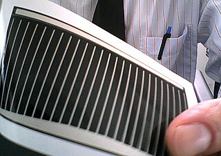
A copper indium gallium selenide solar cell is a thin-film solar cell used to convert sunlight into electric power. It is manufactured by depositing a thin layer of copper, indium, gallium and selenium on glass or plastic backing, along with electrodes on the front and back to collect current. Because the material has a high absorption coefficient and strongly absorbs sunlight, a much thinner film is required than of other semiconductor materials.

Polycrystalline silicon, or multicrystalline silicon, also called polysilicon or poly-Si, is a high purity, polycrystalline form of silicon, used as a raw material by the solar photovoltaic and electronics industry.
A rapidly increasing list of graphene production techniques have been developed to enable graphene's use in commercial applications.
A graphene morphology is any of the structures related to, and formed from, single sheets of graphene. 'Graphene' is typically used to refer to the crystalline monolayer of the naturally occurring material graphite. Due to quantum confinement of electrons within the material at these low dimensions, small differences in graphene morphology can greatly impact the physical and chemical properties of these materials. Commonly studied graphene morphologies include the monolayer sheets, bilayer sheets, graphene nanoribbons and other 3D structures formed from stacking of the monolayer sheets.
Two dimensional hexagonal boron nitride is a material of comparable structure to graphene with potential applications in e.g. photonics., fuel cells and as a substrate for two-dimensional heterostructures. 2D h-BN is isostructural to graphene, but where graphene is conductive, 2D h-BN is a wide-gap insulator.
References
- ↑ "The growth of a polycrystalline graphene from a liquid phase". www.nsti.org. Retrieved 2015-07-01.
- ↑ "Single and Multilayer Growth of Graphene from the Liquid Phase". www.scientific.net. Retrieved 2015-07-01.
- ↑ "Polish scientists find way to make super-strong graphene sheets | Graphene-Info". www.graphene-info.com. Retrieved 2015-07-01.
- ↑ "Engineering graphene : Compute Scotland". www.computescotland.com. Retrieved 2015-07-01.
| | This material-related article is a stub. You can help Wikipedia by expanding it. |