Asynchronous Transfer Mode (ATM) is a telecommunications standard defined by ANSI and ITU for digital transmission of multiple types of traffic, including telephony (voice), data, and video signals in one network without the use of separate overlay networks. ATM was developed to meet the needs of the Broadband Integrated Services Digital Network, as defined in the late 1980s, and designed to integrate telecommunication networks. It can handle both traditional high-throughput data traffic and real-time, low-latency content such as voice and video. ATM provides functionality that uses features of circuit switching and packet switching networks. It uses asynchronous time-division multiplexing, and encodes data into small, fixed-sized network packets.
A central processing unit (CPU), also called a central processor, main processor or just processor, is the electronic circuitry that executes instructions comprising a computer program. The CPU performs basic arithmetic, logic, controlling, and input/output (I/O) operations specified by the instructions in the program. This contrasts with external components such as main memory and I/O circuitry, and specialized processors such as graphics processing units (GPUs).

In computing, a cache is a hardware or software component that stores data so that future requests for that data can be served faster; the data stored in a cache might be the result of an earlier computation or a copy of data stored elsewhere. A cache hit occurs when the requested data can be found in a cache, while a cache miss occurs when it cannot. Cache hits are served by reading data from the cache, which is faster than recomputing a result or reading from a slower data store; thus, the more requests that can be served from the cache, the faster the system performs.

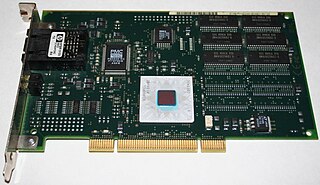
Peripheral Component Interconnect (PCI) is a local computer bus for attaching hardware devices in a computer and is part of the PCI Local Bus standard. The PCI bus supports the functions found on a processor bus but in a standardized format that is independent of any given processor's native bus. Devices connected to the PCI bus appear to a bus master to be connected directly to its own bus and are assigned addresses in the processor's address space. It is a parallel bus, synchronous to a single bus clock. Attached devices can take either the form of an integrated circuit fitted onto the motherboard or an expansion card that fits into a slot. The PCI Local Bus was first implemented in IBM PC compatibles, where it displaced the combination of several slow Industry Standard Architecture (ISA) slots and one fast VESA Local Bus (VLB) slot as the bus configuration. It has subsequently been adopted for other computer types. Typical PCI cards used in PCs include: network cards, sound cards, modems, extra ports such as Universal Serial Bus (USB) or serial, TV tuner cards and hard disk drive host adapters. PCI video cards replaced ISA and VLB cards until rising bandwidth needs outgrew the abilities of PCI. The preferred interface for video cards then became Accelerated Graphics Port (AGP), a superset of PCI, before giving way to PCI Express.
The E-carrier is a member of the series of carrier systems developed for digital transmission of many simultaneous telephone calls by time-division multiplexing. The European Conference of Postal and Telecommunications Administrations (CEPT) originally standardized the E-carrier system, which revised and improved the earlier American T-carrier technology, and this has now been adopted by the International Telecommunication Union Telecommunication Standardization Sector (ITU-T). It was widely adopted in almost all countries outside the US, Canada, and Japan. E-carrier deployments have steadily been replaced by Ethernet as telecommunication networks transitions towards all IP.
Direct memory access (DMA) is a feature of computer systems that allows certain hardware subsystems to access main system memory independent of the central processing unit (CPU).
In computer science, locality of reference, also known as the principle of locality, is the tendency of a processor to access the same set of memory locations repetitively over a short period of time. There are two basic types of reference locality – temporal and spatial locality. Temporal locality refers to the reuse of specific data and/or resources within a relatively small time duration. Spatial locality refers to the use of data elements within relatively close storage locations. Sequential locality, a special case of spatial locality, occurs when data elements are arranged and accessed linearly, such as traversing the elements in a one-dimensional array.
In electronics, a digital-to-analog converter is a system that converts a digital signal into an analog signal. An analog-to-digital converter (ADC) performs the reverse function.
In computing, protected mode, also called protected virtual address mode, is an operational mode of x86-compatible central processing units (CPUs). It allows system software to use features such as virtual memory, paging and safe multi-tasking designed to increase an operating system's control over application software.

A memory management unit (MMU), sometimes called paged memory management unit (PMMU), is a computer hardware unit having all memory references passed through itself, primarily performing the translation of virtual memory addresses to physical addresses.
A translation lookaside buffer (TLB) is a memory cache that is used to reduce the time taken to access a user memory location. It is a part of the chip's memory-management unit (MMU). The TLB stores the recent translations of virtual memory to physical memory and can be called an address-translation cache. A TLB may reside between the CPU and the CPU cache, between CPU cache and the main memory or between the different levels of the multi-level cache. The majority of desktop, laptop, and server processors include one or more TLBs in the memory-management hardware, and it is nearly always present in any processor that utilizes paged or segmented virtual memory.
A CPU cache is a hardware cache used by the central processing unit (CPU) of a computer to reduce the average cost to access data from the main memory. A cache is a smaller, faster memory, located closer to a processor core, which stores copies of the data from frequently used main memory locations. Most CPUs have a hierarchy of multiple cache levels, with separate instruction-specific and data-specific caches at level 1.
In computing, cache algorithms are optimizing instructions, or algorithms, that a computer program or a hardware-maintained structure can utilize in order to manage a cache of information stored on the computer. Caching improves performance by keeping recent or often-used data items in memory locations that are faster or computationally cheaper to access than normal memory stores. When the cache is full, the algorithm must choose which items to discard to make room for the new ones.
The Orion was a series of 32-bit super-minicomputers designed and produced in the 1980s by High Level Hardware Limited (HLH), a company based in Oxford, UK. The company produced four versions of the machine:
The modified Harvard architecture is a variation of the Harvard computer architecture that, unlike the pure Harvard architecture, allows the contents of the instruction memory to be accessed as data. Most modern computers that are documented as Harvard architecture are, in fact, modified Harvard architecture.
This glossary of computer hardware terms is a list of definitions of terms and concepts related to computer hardware, i.e. the physical and structural components of computers, architectural issues, and peripheral devices.
Bus encoding refers to converting/encoding a piece of data to another form before launching on the bus. While bus encoding can be used to serve various purposes like reducing the number of pins, compressing the data to be transmitted, reducing cross-talk between bit lines, etc., it is one of the popular techniques used in system design to reduce dynamic power consumed by the system bus. Bus encoding aims to reduce the Hamming distance between 2 consecutive values on the bus. Since the activity is directly proportional to the Hamming distance, bus encoding proves to be effective in reducing the overall activity factor thereby reducing the dynamic power consumption in the system.
Power consumption is becoming increasingly important for both embedded, mobile computing and high-performance systems. Off-chip data bus consumes a significant part of system power. It is observed that the off-chip data bus consumes between 9.8% and 23.2% of the total power consumed by the system depending on the system. So, reducing the power consumption of the off-chip data bus would reduce the overall power consumption.
A CPU cache is a memory which holds the recently utilized data by the processor. A block of memory cannot necessarily be placed randomly in the cache and may be restricted to a single cache line or a set of cache lines by the cache placement policy. In other words, the cache placement policy determines where a particular memory block can be placed when it goes into the cache.

Cache hierarchy, or multi-level caches, refers to a memory architecture that uses a hierarchy of memory stores based on varying access speeds to cache data. Highly-requested data is cached in high-speed access memory stores, allowing swifter access by central processing unit (CPU) cores.