
Chemical vapor deposition (CVD) is a vacuum deposition method used to produce high quality, and high-performance, solid materials. The process is often used in the semiconductor industry to produce thin films.

Gallium arsenide (GaAs) is a III-V direct band gap semiconductor with a zinc blende crystal structure.

Epitaxy refers to a type of crystal growth or material deposition in which new crystalline layers are formed with one or more well-defined orientations with respect to the crystalline seed layer. The deposited crystalline film is called an epitaxial film or epitaxial layer. The relative orientation(s) of the epitaxial layer to the seed layer is defined in terms of the orientation of the crystal lattice of each material. For most epitaxial growths, the new layer is usually crystalline and each crystallographic domain of the overlayer must have a well-defined orientation relative to the substrate crystal structure. Epitaxy can involve single-crystal structures, although grain-to-grain epitaxy has been observed in granular films. For most technological applications, single domain epitaxy, which is the growth of an overlayer crystal with one well-defined orientation with respect to the substrate crystal, is preferred. Epitaxy can also play an important role while growing superlattice structures.

Molecular-beam epitaxy (MBE) is an epitaxy method for thin-film deposition of single crystals. MBE is widely used in the manufacture of semiconductor devices, including transistors, and it is considered one of the fundamental tools for the development of nanotechnologies. MBE is used to fabricate diodes and MOSFETs at microwave frequencies, and to manufacture the lasers used to read optical discs.
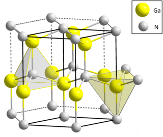
Gallium nitride is a binary III/V direct bandgap semiconductor commonly used in blue light-emitting diodes since the 1990s. The compound is a very hard material that has a Wurtzite crystal structure. Its wide band gap of 3.4 eV affords it special properties for applications in optoelectronic, high-power and high-frequency devices. For example, GaN is the substrate which makes violet (405 nm) laser diodes possible, without requiring nonlinear optical frequency-doubling.
An epitaxial wafer is a wafer of semiconducting material made by epitaxial growth (epitaxy) for use in photonics, microelectronics, spintronics, or photovoltaics. The epi layer may be the same material as the substrate, typically monocrystaline silicon, or it may be a more exotic material with specific desirable qualities.
Indium gallium arsenide (InGaAs) is a ternary alloy of indium arsenide (InAs) and gallium arsenide (GaAs). Indium and gallium are elements of the periodic table while arsenic is a element. Alloys made of these chemical groups are referred to as "III-V" compounds. InGaAs has properties intermediate between those of GaAs and InAs. InGaAs is a room-temperature semiconductor with applications in electronics and photonics.
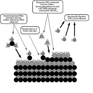
Metalorganic vapour-phase epitaxy (MOVPE), also known as organometallic vapour-phase epitaxy (OMVPE) or metalorganic chemical vapour deposition (MOCVD), is a chemical vapour deposition method used to produce single- or polycrystalline thin films. It is a process for growing crystalline layers to create complex semiconductor multilayer structures. In contrast to molecular-beam epitaxy (MBE), the growth of crystals is by chemical reaction and not physical deposition. This takes place not in vacuum, but from the gas phase at moderate pressures. As such, this technique is preferred for the formation of devices incorporating thermodynamically metastable alloys, and it has become a major process in the manufacture of optoelectronics, such as Light-emitting diodes. It was invented in 1968 at North American Aviation Science Center by Harold M. Manasevit.

Germane is the chemical compound with the formula GeH4, and the germanium analogue of methane. It is the simplest germanium hydride and one of the most useful compounds of germanium. Like the related compounds silane and methane, germane is tetrahedral. It burns in air to produce GeO2 and water. Germane is a group 14 hydride.
Chemical beam epitaxy (CBE) forms an important class of deposition techniques for semiconductor layer systems, especially III-V semiconductor systems. This form of epitaxial growth is performed in an ultrahigh vacuum system. The reactants are in the form of molecular beams of reactive gases, typically as the hydride or a metalorganic. The term CBE is often used interchangeably with metal-organic molecular beam epitaxy (MOMBE). The nomenclature does differentiate between the two processes, however. When used in the strictest sense, CBE refers to the technique in which both components are obtained from gaseous sources, while MOMBE refers to the technique in which the group III component is obtained from a gaseous source and the group V component from a solid source.

Zinc nitride (Zn3N2) is an inorganic compound of zinc and nitrogen, usually obtained as (blue)grey crystals. It is a semiconductor. In pure form, it has the anti-bixbyite structure.
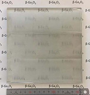
Gallium(III) trioxide is an inorganic compound with the formula Ga2O3. It exists as several polymorphs, all of which are white, water-insoluble solids. Although no commercial applications exist, Ga2O3 is an intermediate in the purification of gallium, which is consumed almost exclusively as gallium arsenide. The thermal conductivity of β-Ga2O3 is at least one order of magnitude lower than the other wide bandgap semiconductors, such as GaN and SiC. It is further reduced for related nanostructures which are usually used in electronic devices. Heterogeneous integration with high thermal conductivity substrates such as diamond and SiC helps heat dissipation of β-Ga2O3 electronics.
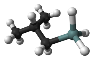
Isobutylgermane (IBGe, Chemical formula: (CH3)2CHCH2GeH3, is an organogermanium compound. It is a colourless, volatile liquid that is used in MOVPE (Metalorganic Vapor Phase Epitaxy) as an alternative to germane. IBGe is used in the deposition of Ge films and Ge-containing thin semiconductor films such as SiGe in strained silicon application, and GeSbTe in NAND Flash applications.

Dichlorosilane, or DCS as it is commonly known, is a chemical compound with the formula H2SiCl2. In its major use, it is mixed with ammonia (NH3) in LPCVD chambers to grow silicon nitride in semiconductor processing. A higher concentration of DCS·NH3 (i.e. 16:1), usually results in lower stress nitride films.
A micropipe, also called a micropore, microtube, capillary defect or pinhole defect, is a crystallographic defect in a single crystal substrate. Minimizing the presence of micropipes is important in semiconductor manufacturing, as their presence on a wafer can result in the failure of integrated circuits made from that wafer.
Selective area epitaxy is the local growth of epitaxial layer through a patterned amorphous dielectric mask (typically SiO2 or Si3N4) deposited on a semiconductor substrate. Semiconductor growth conditions are selected to ensure epitaxial growth on the exposed substrate, but not on the dielectric mask. SAE can be executed in various epitaxial growth methods such as molecular beam epitaxy (MBE), metalorganic vapour phase epitaxy (MOVPE) and chemical beam epitaxy (CBE). By SAE, semiconductor nanostructures such as quantum dots and nanowires can be grown to their designed places.
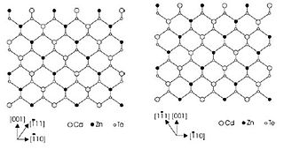
One of the most studied atomic ordering is CuPt type ordering in III-V semiconductor alloy in chemistry and physics. It occurs in III-V alloy when the cation planes take an alternate sequence of A-rich and B-rich plane following AxB1−xC. The resulting structure is usually called as superlattice-like structure along [1-11] or [-111] – called (111) B plane, or along [-1-1-1] or [11-1] – called (111) A plane. The two ordering direction is thus called CuPt type A and B ordering.
IQE is a British semiconductor company founded 1988 in Cardiff, Wales, which manufactures advanced epitaxial wafers for a wide range of technology applications for wireless, optoelectronic, electronic and solar devices. IQE specialises in advanced silicon and compound semiconductor materials based on gallium arsenide (GaAs), indium phosphide (InP), gallium nitride (GaN) and silicon. The company is the largest independent outsource producer of epiwafers manufactured by metalorganic vapour phase epitaxy (MOCVD), molecular beam epitaxy (MBE) and chemical vapor deposition (CVD).
Indium aluminium nitride (InAlN) is a direct bandgap semiconductor material used in the manufacture of electronic and photonic devices. It is part of the III-V group of semiconductors, being an alloy of indium nitride and aluminium nitride, and is closely related to the more widely used gallium nitride. It is of special interest in applications requiring good stability and reliability, owing to its large direct bandgap and ability to maintain operation at temperatures of up to 1000 °C., making it of particular interest to areas such as the space industry. InAlN high-electron-mobility transistors (HEMTs) are attractive candidates for such applications owing to the ability of InAlN to lattice-match to gallium nitride, eliminating a reported failure route in the closely related aluminium gallium nitride HEMTs.

Vladimir G. Dubrovskii is the head of Laboratory of physics of nanostructures at St. Petersburg Academic University, a leading research scientist at Ioffe Institute, and a professor at St. Petersburg State University and ITMO University.