Related Research Articles
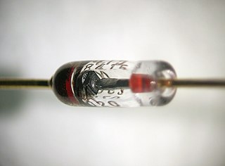
A diode is a two-terminal electronic component that conducts current primarily in one direction ; it has low resistance in one direction, and high resistance in the other. A diode vacuum tube or thermionic diode is a vacuum tube with two electrodes, a heated cathode and a plate, in which electrons can flow in only one direction, from cathode to plate. A semiconductor diode, the most commonly used type today, is a crystalline piece of semiconductor material with a p–n junction connected to two electrical terminals. Semiconductor diodes were the first semiconductor electronic devices. The discovery of asymmetric electrical conduction across the contact between a crystalline mineral and a metal was made by German physicist Ferdinand Braun in 1874. Today, most diodes are made of silicon, but other semiconducting materials such as gallium arsenide and germanium are also used.

A microscope is a laboratory instrument used to examine objects that are too small to be seen by the naked eye. Microscopy is the science of investigating small objects and structures using a microscope. Microscopic means being invisible to the eye unless aided by a microscope.

A multimeter is a measuring instrument that can measure multiple electrical properties. A typical multimeter can measure voltage, resistance, and current, in which case it is also known as a volt-ohm-milliammeter (VOM), as the unit is equipped with voltmeter, ammeter, and ohmmeter functionality. Some feature the measurement of additional properties such as temperature and volume.

A time-domain reflectometer (TDR) is an electronic instrument used to determine the characteristics of electrical lines by observing reflected waveforms.

Photonics is the physical science and application of light (photon) generation, detection, and manipulation through emission, transmission, modulation, signal processing, switching, amplification, and sensing. Though covering all light's technical applications over the whole spectrum, most photonic applications are in the range of visible and near-infrared light. The term photonics developed as an outgrowth of the first practical semiconductor light emitters invented in the early 1960s and optical fibers developed in the 1970s.
A transducer is a device that converts energy from one form to another. Usually a transducer converts a signal in one form of energy to a signal in another.

Ellipsometry is an optical technique for investigating the dielectric properties of thin films. Ellipsometry measures the change of polarization upon reflection or transmission and compares it to a model.

Photodetectors, also called photosensors, are sensors of light or other electromagnetic radiation. There is a wide variety of photodetectors which may be classified by mechanism of detection, such as photoelectric or photochemical effects, or by various performance metrics, such as spectral response. Semiconductor-based photodetectors typically have a p–n junction that converts light photons into current. The absorbed photons make electron–hole pairs in the depletion region. Photodiodes and phototransistors are a few examples of photodetectors. Solar cells convert some of the light energy absorbed into electrical energy.

Automatic test equipment or automated test equipment (ATE) is any apparatus that performs tests on a device, known as the device under test (DUT), equipment under test (EUT) or unit under test (UUT), using automation to quickly perform measurements and evaluate the test results. An ATE can be a simple computer-controlled digital multimeter, or a complicated system containing dozens of complex test instruments capable of automatically testing and diagnosing faults in sophisticated electronic packaged parts or on wafer testing, including system on chips and integrated circuits.
The grating light valve (GLV) is a "micro projection" technology which operates using a dynamically adjustable diffraction grating. It competes with other light valve technologies such as Digital Light Processing (DLP) and liquid crystal on silicon (LCoS) for implementation in video projector devices such as rear-projection televisions. The use of microelectromechanical systems (MEMS) in optical applications, which is known as optical MEMS or micro-opto-electro-mechanical structures (MOEMS), has enabled the possibility to combine the mechanical, electrical and optical components in very small scale.
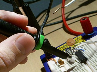
A test probe is a physical device used to connect electronic test equipment to a device under test (DUT). Test probes range from very simple, robust devices to complex probes that are sophisticated, expensive, and fragile. Specific types include test prods, oscilloscope probes and current probes. A test probe is often supplied as a test lead, which includes the probe, cable and terminating connector.
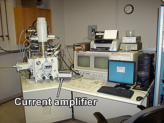
Electron-beam-induced current (EBIC) is a semiconductor analysis technique performed in a scanning electron microscope (SEM) or scanning transmission electron microscope (STEM). It is used to identify buried junctions or defects in semiconductors, or to examine minority carrier properties. EBIC is similar to cathodoluminescence in that it depends on the creation of electron–hole pairs in the semiconductor sample by the microscope's electron beam. This technique is used in semiconductor failure analysis and solid-state physics.
The electron beam prober is a specialized adaption of a standard scanning electron microscope (SEM) that is used for semiconductor failure analysis. While a conventional SEM may be operated in a voltage range of 10–30 keV, the e-beam Prober typically operates at 1 keV. The e-beam prober is capable of measuring voltage and timing waveforms on internal semiconductor signal structures. Waveforms may be measured on metal line, polysilicon and diffusion structures that have an electrically active, changing signal. The operation of the prober is similar to that of a sampling oscilloscope. A continuously looping, repeating test pattern must be applied to the device-under-test (DUT). E-beam probers are used primarily for front side semiconductor analysis. With the advent of flip-chip technology, many e-beam probers have been replaced with back side analysis instruments.
Time-resolved photon emission (TRPE) is used to measure timing waveforms on semiconductor devices. TRPE measurements are performed on the back side of the semiconductor device. The substrate of the device-under-test (DUT) must first be thinned mechanically. The device is mounted on a movable X-Y stage in an enclosure which shields it from all sources of light. The DUT is connected to an active electrical stimulus. The stimulus pattern is continuously looped and a trigger signal is sent to the TRPE instrument in order to tell it when the pattern repeats. A TRPE prober operates in a manner similar to a sampling oscilloscope, and is used to perform semiconductor failure analysis.

Ultrasonic transducers and ultrasonic sensors are devices that generate or sense ultrasound energy. They can be divided into three broad categories: transmitters, receivers and transceivers. Transmitters convert electrical signals into ultrasound, receivers convert ultrasound into electrical signals, and transceivers can both transmit and receive ultrasound.

An oscilloscope, previously called an oscillograph, and informally known as a scope or o-scope, CRO, or DSO, is a type of electronic test instrument that graphically displays varying signal voltages, usually as a calibrated two-dimensional plot of one or more signals as a function of time. The displayed waveform can then be analyzed for properties such as amplitude, frequency, rise time, time interval, distortion, and others. Originally, calculation of these values required manually measuring the waveform against the scales built into the screen of the instrument. Modern digital instruments may calculate and display these properties directly.
This is a subdivision of the Oscilloscope article, discussing the various types and models of oscilloscopes in greater detail.

A measuring instrument is a device to measure a physical quantity. In the physical sciences, quality assurance, and engineering, measurement is the activity of obtaining and comparing physical quantities of real-world objects and events. Established standard objects and events are used as units, and the process of measurement gives a number relating the item under study and the referenced unit of measurement. Measuring instruments, and formal test methods which define the instrument's use, are the means by which these relations of numbers are obtained. All measuring instruments are subject to varying degrees of instrument error and measurement uncertainty. These instruments may range from simple objects such as rulers and stopwatches to electron microscopes and particle accelerators. Virtual instrumentation is widely used in the development of modern measuring instruments.

Photoconductive atomic force microscopy (PC-AFM) is a variant of atomic force microscopy that measures photoconductivity in addition to surface forces.
Most of the terms listed in Wikipedia glossaries are already defined and explained within Wikipedia itself. However, glossaries like this one are useful for looking up, comparing and reviewing large numbers of terms together. You can help enhance this page by adding new terms or writing definitions for existing ones.
References
- Kolachina, S. (2004). "Introduction to Laser Voltage Probing (LVP) of Integrated Circuits". Microelectronics Failure Analysis. ASM International. pp. 426–430. ISBN 0-87170-804-3.