
A microscope is a laboratory instrument used to examine objects that are too small to be seen by the naked eye. Microscopy is the science of investigating small objects and structures using a microscope. Microscopic means being invisible to the eye unless aided by a microscope.
Differential scanning calorimetry (DSC) is a thermoanalytical technique in which the difference in the amount of heat required to increase the temperature of a sample and reference is measured as a function of temperature. Both the sample and reference are maintained at nearly the same temperature throughout the experiment. Generally, the temperature program for a DSC analysis is designed such that the sample holder temperature increases linearly as a function of time. The reference sample should have a well-defined heat capacity over the range of temperatures to be scanned. Additionally, the reference sample must be stable, of high purity, and must not experience much change across the temperature scan. Typically, reference standards have been metals such as indium, tin, bismuth, and lead, but other standards such as polyethylene and fatty acids have been proposed to study polymers and organic compounds, respectively.

Atomic force microscopy (AFM) or scanning force microscopy (SFM) is a very-high-resolution type of scanning probe microscopy (SPM), with demonstrated resolution on the order of fractions of a nanometer, more than 1000 times better than the optical diffraction limit.
Thermal analysis is a branch of materials science where the properties of materials are studied as they change with temperature. Several methods are commonly used – these are distinguished from one another by the property which is measured:
Scanning probe microscopy (SPM) is a branch of microscopy that forms images of surfaces using a physical probe that scans the specimen. SPM was founded in 1981, with the invention of the scanning tunneling microscope, an instrument for imaging surfaces at the atomic level. The first successful scanning tunneling microscope experiment was done by Gerd Binnig and Heinrich Rohrer. The key to their success was using a feedback loop to regulate gap distance between the sample and the probe.
A microprobe is an instrument that applies a stable and well-focused beam of charged particles to a sample.
Surface metrology is the measurement of small-scale features on surfaces, and is a branch of metrology. Surface primary form, surface fractality, and surface finish are the parameters most commonly associated with the field. It is important to many disciplines and is mostly known for the machining of precision parts and assemblies which contain mating surfaces or which must operate with high internal pressures.

Focused ion beam, also known as FIB, is a technique used particularly in the semiconductor industry, materials science and increasingly in the biological field for site-specific analysis, deposition, and ablation of materials. A FIB setup is a scientific instrument that resembles a scanning electron microscope (SEM). However, while the SEM uses a focused beam of electrons to image the sample in the chamber, a FIB setup uses a focused beam of ions instead. FIB can also be incorporated in a system with both electron and ion beam columns, allowing the same feature to be investigated using either of the beams. FIB should not be confused with using a beam of focused ions for direct write lithography. These are generally quite different systems where the material is modified by other mechanisms.

Near-field scanning optical microscopy (NSOM) or scanning near-field optical microscopy (SNOM) is a microscopy technique for nanostructure investigation that breaks the far field resolution limit by exploiting the properties of evanescent waves. In SNOM, the excitation laser light is focused through an aperture with a diameter smaller than the excitation wavelength, resulting in an evanescent field on the far side of the aperture. When the sample is scanned at a small distance below the aperture, the optical resolution of transmitted or reflected light is limited only by the diameter of the aperture. In particular, lateral resolution of 6 nm and vertical resolution of 2–5 nm have been demonstrated.
Scanning capacitance microscopy (SCM) is a variety of scanning probe microscopy in which a narrow probe electrode is positioned in contact or close proximity of a sample's surface and scanned. SCM characterizes the surface of the sample using information obtained from the change in electrostatic capacitance between the surface and the probe.
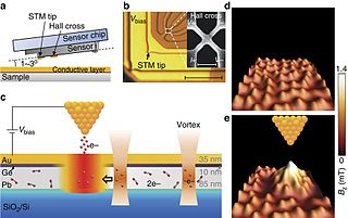
Scanning Hall probe microscope (SHPM) is a variety of a scanning probe microscope which incorporates accurate sample approach and positioning of the scanning tunnelling microscope with a semiconductor Hall sensor. Developed in 1996 by Oral, Bending and Henini, SHPM allows mapping the magnetic induction associated with a sample. Current state of the art SHPM systems utilize 2D electron gas materials to provide high spatial resolution (~300 nm) imaging with high magnetic field sensitivity. Unlike the magnetic force microscope the SHPM provides direct quantitative information on the magnetic state of a material. The SHPM can also image magnetic induction under applied fields up to ~1 tesla and over a wide range of temperatures.
Photothermal microspectroscopy (PTMS), alternatively known as photothermal temperature fluctuation (PTTF), is derived from two parent instrumental techniques: infrared spectroscopy and atomic force microscopy (AFM). In one particular type of AFM, known as scanning thermal microscopy (SThM), the imaging probe is a sub-miniature temperature sensor, which may be a thermocouple or a resistance thermometer. This same type of detector is employed in a PTMS instrument, enabling it to provide AFM/SThM images: However, the chief additional use of PTMS is to yield infrared spectra from sample regions below a micrometer, as outlined below.
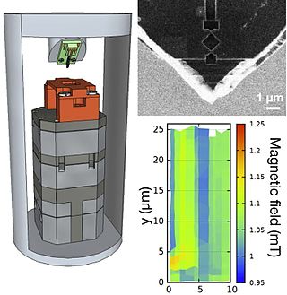
In condensed matter physics, scanning SQUID microscopy is a technique where a superconducting quantum interference device (SQUID) is used to image surface magnetic field strength with micrometre-scale resolution. A tiny SQUID is mounted onto a tip which is then rastered near the surface of the sample to be measured. As the SQUID is the most sensitive detector of magnetic fields available and can be constructed at submicrometre widths via lithography, the scanning SQUID microscope allows magnetic fields to be measured with unparalleled resolution and sensitivity. The first scanning SQUID microscope was built in 1992 by Black et al. Since then the technique has been used to confirm unconventional superconductivity in several high-temperature superconductors including YBCO and BSCCO compounds.

Scanning thermal microscopy (SThM) is a type of scanning probe microscopy that maps the local temperature and thermal conductivity of an interface. The probe in a scanning thermal microscope is sensitive to local temperatures – providing a nano-scale thermometer. Thermal measurements at the nanometer scale are of both scientific and industrial interest. The technique was invented by Clayton C. Williams and H. Kumar Wickramasinghe in 1986.
In microscopy, scanning joule expansion microscopy (SJEM) is a form of scanning probe microscopy heavily based on atomic force microscopy (AFM) that maps the temperature distribution along a surface. Resolutions down to 10 nm have been achieved and 1 nm resolution is theoretically possible. Thermal measurements at the nanometer scale are of both academic and industrial interest, particularly in regards to nanomaterials and modern integrated circuits.
The technique of vibrational analysis with scanning probe microscopy allows probing vibrational properties of materials at the submicrometer scale, and even of individual molecules. This is accomplished by integrating scanning probe microscopy (SPM) and vibrational spectroscopy. This combination allows for much higher spatial resolution than can be achieved with conventional Raman/FTIR instrumentation. The technique is also nondestructive, requires non-extensive sample preparation, and provides more contrast such as intensity contrast, polarization contrast and wavelength contrast, as well as providing specific chemical information and topography images simultaneously.
Scanning electrochemical microscopy (SECM) is a technique within the broader class of scanning probe microscopy (SPM) that is used to measure the local electrochemical behavior of liquid/solid, liquid/gas and liquid/liquid interfaces. Initial characterization of the technique was credited to University of Texas electrochemist, Allen J. Bard, in 1989. Since then, the theoretical underpinnings have matured to allow widespread use of the technique in chemistry, biology and materials science. Spatially resolved electrochemical signals can be acquired by measuring the current at an ultramicroelectrode (UME) tip as a function of precise tip position over a substrate region of interest. Interpretation of the SECM signal is based on the concept of diffusion-limited current. Two-dimensional raster scan information can be compiled to generate images of surface reactivity and chemical kinetics.
AFM-IR or infrared nanospectroscopy is one of a family of techniques that are derived from a combination of two parent instrumental techniques. AFM-IR combines the chemical analysis power of infrared spectroscopy and the high-spatial resolution of scanning probe microscopy (SPM). The term was first used to denote a method that combined a tuneable free electron laser with an atomic force microscope equipped with a sharp probe that measured the local absorption of infrared light by a sample with nanoscale spatial resolution.
A probe tip is an instrument used in scanning probe microscopes (SPMs) to scan the surface of a sample and make nano-scale images of surfaces and structures. The probe tip is mounted on the end of a cantilever and can be as sharp as a single atom. In microscopy, probe tip geometry and the composition of both the tip and the surface being probed directly affect resolution and imaging quality. Tip size and shape are extremely important in monitoring and detecting interactions between surfaces. SPMs can precisely measure electrostatic forces, magnetic forces, chemical bonding, Van der Waals forces, and capillary forces. SPMs can also reveal the morphology and topography of a surface.

Multi-tip scanning tunneling microscopy extends scanning tunneling microscopy (STM) from imaging to dedicated electrical measurements at the nanoscale like a ″multimeter at the nanoscale″. In materials science, nanoscience, and nanotechnology, it is desirable to measure electrical properties at a particular position of the sample. For this purpose, multi-tip STMs in which several tips are operated independently have been developed. Apart from imaging the sample, the tips of a multi-tip STM are used to form contacts to the sample at desired locations and to perform local electrical measurements.