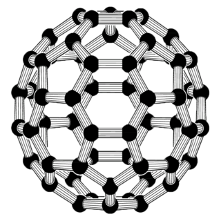
Nanomaterials describe, in principle, materials of which a single unit is sized between 1 to 1000 nanometres but usually is 1 to 100 nm.

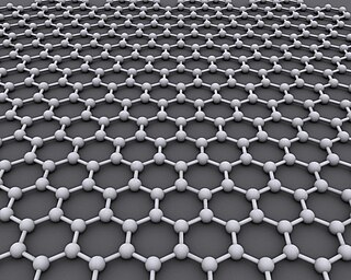
Graphene (/ˈɡræfiːn/) is an allotrope of carbon in the form of a single layer of atoms in a two-dimensional hexagonal lattice in which one atom forms each vertex. It is the basic structural element of other allotropes, including graphite, charcoal, carbon nanotubes and fullerenes. It can also be considered as an indefinitely large aromatic molecule, the ultimate case of the family of flat polycyclic aromatic hydrocarbons.
A "photoelectrochemical cell" is one of two distinct classes of device. The first produces electrical energy similarly to a dye-sensitized photovoltaic cell, which meets the standard definition of a photovoltaic cell. The second is a photoelectrolytic cell, that is, a device which uses light incident on a photosensitizer, semiconductor, or aqueous metal immersed in an electrolytic solution to directly cause a chemical reaction, for example to produce hydrogen via the electrolysis of water.

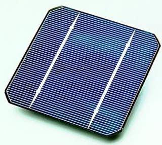
A solar cell, or photovoltaic cell, is an electrical device that converts the energy of light directly into electricity by the photovoltaic effect, which is a physical and chemical phenomenon. It is a form of photoelectric cell, defined as a device whose electrical characteristics, such as current, voltage, or resistance, vary when exposed to light. Individual solar cell devices can be combined to form modules, otherwise known as solar panels. In basic terms a single junction silicon solar cell can produce a maximum open-circuit voltage of approximately 0.5 to 0.6 volts.
Hybrid solar cells combine advantages of both organic and inorganic semiconductors. Hybrid photovoltaics have organic materials that consist of conjugated polymers that absorb light as the donor and transport holes. Inorganic materials in hybrid cells are used as the acceptor and electron transporter in the structure. The hybrid photovoltaic devices have a potential for not only low-cost by roll-to-roll processing but also for scalable solar power conversion.

A gyroid is an infinitely connected triply periodic minimal surface discovered by Alan Schoen in 1970.
Nanochemistry is the combination of chemistry and nanoscience. Nanochemistry is associated with synthesis of building blocks which are dependent on size, surface, shape and defect properties. Nanochemistry is being used in chemical, materials and physical, science as well as engineering, biological and medical applications. Nanochemistry and other nanoscience fields have the same core concepts but the usages of those concepts are different.

Nanofluidics is the study of the behavior, manipulation, and control of fluids that are confined to structures of nanometer characteristic dimensions. Fluids confined in these structures exhibit physical behaviors not observed in larger structures, such as those of micrometer dimensions and above, because the characteristic physical scaling lengths of the fluid, very closely coincide with the dimensions of the nanostructure itself.
Over the past few decades, the fields of science and engineering have been seeking to develop new and improved types of energy technologies that have the capability of improving life all over the world. In order to make the next leap forward from the current generation of technology, scientists and engineers have been developing energy applications of nanotechnology. Nanotechnology, a new field in science, is any technology that contains components smaller than 100 nanometers. For scale, a single virus particle is about 100 nanometers in width.
A biointerface is the region of contact between a biomolecule, cell, biological tissue or living organism or organic material considered living with another biomaterial or inorganic/organic material. The motivation for biointerface science stems from the urgent need to increase the understanding of interactions between biomolecules and surfaces. The behavior of complex macromolecular systems at materials interfaces are important in the fields of biology, biotechnology, diagnostics, and medicine. Biointerface science is a multidisciplinary field in which (bio)chemists who synthesize novel classes of biomolecules cooperate with scientists who have developed the tools to position biomolecules with molecular precision, scientists who have developed new spectroscopic techniques to interrogate these molecules at the solid-liquid interface, and people who integrate these into functional devices.
A nanowire battery uses nanowires to increase the surface area of one or both of its electrodes. Some designs, variations of the lithium-ion battery have been announced, although none are commercially available. All of the concepts replace the traditional graphite anode and could improve battery performance.
Organic photovoltaic devices (OPVs) are fabricated from thin films of organic semiconductors, such as polymers and small-molecule compounds, and are typically on the order of 100 nm thick. Because polymer based OPVs can be made using a coating process such as spin coating or inkjet printing, they are an attractive option for inexpensively covering large areas as well as flexible plastic surfaces. A promising low cost alternative to conventional solar cells made of crystalline silicon, there is a large amount of research being dedicated throughout industry and academia towards developing OPVs and increasing their power conversion efficiency.
Nanoarchitectures for lithium-ion batteries are attempts to employ nanotechnology to improve the design of lithium-ion batteries. Research in lithium-ion batteries focuses on improving energy density, power density, safety, durability and cost.
A plasmonic-enhanced solar cell, commonly referred to simply as plasmonic solar cell, is a type of solar cell that converts light into electricity with the assistance of plasmons, but where the photovoltaic effect occurs in another material.
A metamaterial absorber is a type of metamaterial intended to efficiently absorb electromagnetic radiation such as light. Furthermore, metamaterials are an advance in materials science. Hence, those metamaterials that are designed to be absorbers offer benefits over conventional absorbers such as further miniaturization, wider adaptability, and increased effectiveness. Intended applications for the metamaterial absorber include emitters, photodetectors, sensors, spatial light modulators, infrared camouflage, wireless communication, and use in solar photovoltaics and thermophotovoltaics.
A holographic sensor is a device that comprises a hologram embedded in a smart material that detects certain molecules or metabolites. This detection is usually a chemical interaction that is transduced as a change in one of the properties of the holographic reflection, either refractive index or spacing between the holographic fringes. The specificity of the sensor can be controlled by adding molecules in the polymer film that selectively interacts with the molecules of interest.
A plasmonic metamaterial is a metamaterial that uses surface plasmons to achieve optical properties not seen in nature. Plasmons are produced from the interaction of light with metal-dielectric materials. Under specific conditions, the incident light couples with the surface plasmons to create self-sustaining, propagating electromagnetic waves known as surface plasmon polaritons (SPPs). Once launched, the SPPs ripple along the metal-dielectric interface. Compared with the incident light, the SPPs can be much shorter in wavelength.
Silicon nanowires, also referred to as SiNWs, are a type of semiconductor nanowire most often formed from a silicon precursor by etching of a solid or through catalyzed growth from a vapor or liquid phase. Such nanowires have promising applications in lithium ion batteries, thermoelectrics and sensors. Initial synthesis of SiNWs is often accompanied by thermal oxidation steps to yield structures of accurately tailored size and morphology.
Graphene is a 2D nanosheet with atomic thin thickness in terms of 0.34 nm. Due to the ultrathin thickness, graphene showed many properties that are quite different from their bulk graphite counterparts. The most prominent advantages are known to be their high electron mobility and high mechanical strengths. Thus, it exhibits potential for applications in optics and electronics especially for the development of wearable devices as flexible substrates. More importantly, the optical absorption rate of graphene is 2.3% in the visible and near-infrared region. This broadband absorption characteristic also attracted great attention of the research community to exploit the graphene-based photodetectors/modulators.

