In physics, sputtering is a phenomenon in which microscopic particles of a solid material are ejected from its surface, after the material is itself bombarded by energetic particles of a plasma or gas. It occurs naturally in outer space, and can be an unwelcome source of wear in precision components. However, the fact that it can be made to act on extremely fine layers of material is utilised in science and industry—there, it is used to perform precise etching, carry out analytical techniques, and deposit thin film layers in the manufacture of optical coatings, semiconductor devices and nanotechnology products. It is a physical vapor deposition technique.
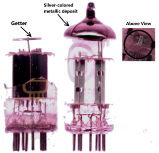
A getter is a deposit of reactive material that is placed inside a vacuum system to complete and maintain the vacuum. When gas molecules strike the getter material, they combine with it chemically or by adsorption. Thus the getter removes small amounts of gas from the evacuated space. The getter is usually a coating applied to a surface within the evacuated chamber.

Pulsed laser deposition (PLD) is a physical vapor deposition (PVD) technique where a high-power pulsed laser beam is focused inside a vacuum chamber to strike a target of the material that is to be deposited. This material is vaporized from the target which deposits it as a thin film on a substrate. This process can occur in ultra high vacuum or in the presence of a background gas, such as oxygen which is commonly used when depositing oxides to fully oxygenate the deposited films.
A thin film is a layer of materials ranging from fractions of a nanometer (monolayer) to several micrometers in thickness. The controlled synthesis of materials as thin films is a fundamental step in many applications. A familiar example is the household mirror, which typically has a thin metal coating on the back of a sheet of glass to form a reflective interface. The process of silvering was once commonly used to produce mirrors, while more recently the metal layer is deposited using techniques such as sputtering. Advances in thin film deposition techniques during the 20th century have enabled a wide range of technological breakthroughs in areas such as magnetic recording media, electronic semiconductor devices, integrated passive devices, light-emitting diodes, optical coatings, hard coatings on cutting tools, and for both energy generation and storage. It is also being applied to pharmaceuticals, via thin-film drug delivery. A stack of thin films is called a multilayer.
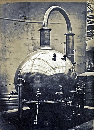
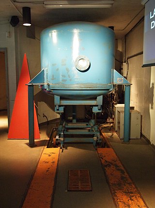
Ultra-high vacuum is the vacuum regime characterised by pressures lower than about 1×10⁻⁶ pascals. UHV conditions are created by pumping the gas out of a UHV chamber. At these low pressures the mean free path of a gas molecule is greater than approximately 40 km, so the gas is in free molecular flow, and gas molecules will collide with the chamber walls many times before colliding with each other. Almost all molecular interactions therefore take place on various surfaces in the chamber.

Metallizing is the general name for the technique of coating metal on the surface of objects. Metallic coatings may be decorative, protective or functional.
Titanium nitride is an extremely hard ceramic material, often used as a physical vapor deposition (PVD) coating on titanium alloys, steel, carbide, and aluminium components to improve the substrate's surface properties.

Ion plating (IP) is a physical vapor deposition (PVD) process that is sometimes called ion assisted deposition (IAD) or ion vapor deposition (IVD) and is a modified version of vacuum deposition. Ion plating uses concurrent or periodic bombardment of the substrate, and deposits film by atomic-sized energetic particles called ions. Bombardment prior to deposition is used to sputter clean the substrate surface. During deposition the bombardment is used to modify and control the properties of the depositing film. It is important that the bombardment be continuous between the cleaning and the deposition portions of the process to maintain an atomically clean interface. If this interface is not properly cleaned, then it can result into a weaker coating or poor adhesion.
Vacuum evaporation is the process of causing the pressure in a liquid-filled container to be reduced below the vapor pressure of the liquid, causing the liquid to evaporate at a lower temperature than normal. Although the process can be applied to any type of liquid at any vapor pressure, it is generally used to describe the boiling of water by lowering the container's internal pressure below standard atmospheric pressure and causing the water to boil at room temperature.
Electron-beam physical vapor deposition, or EBPVD, is a form of physical vapor deposition in which a target anode is bombarded with an electron beam given off by a charged tungsten filament under high vacuum. The electron beam causes atoms from the target to transform into the gaseous phase. These atoms then precipitate into solid form, coating everything in the vacuum chamber with a thin layer of the anode material.

Tantalum nitride (TaN) is a chemical compound, a nitride of tantalum. There are multiple phases of compounds, stoichimetrically from Ta2N to Ta3N5, including TaN.
Vacuum deposition is a group of processes used to deposit layers of material atom-by-atom or molecule-by-molecule on a solid surface. These processes operate at pressures well below atmospheric pressure. The deposited layers can range from a thickness of one atom up to millimeters, forming freestanding structures. Multiple layers of different materials can be used, for example to form optical coatings. The process can be qualified based on the vapor source; physical vapor deposition uses a liquid or solid source and chemical vapor deposition uses a chemical vapor.
Physical vapor deposition (PVD), sometimes called physical vapor transport (PVT), describes a variety of vacuum deposition methods which can be used to produce thin films and coatings on substrates including metals, ceramics, glass, and polymers. PVD is characterized by a process in which the material transitions from a condensed phase to a vapor phase and then back to a thin film condensed phase. The most common PVD processes are sputtering and evaporation. PVD is used in the manufacturing of items which require thin films for optical, mechanical, electrical, acoustic or chemical functions. Examples include semiconductor devices such as thin-film solar cells, microelectromechanical devices such as thin film bulk acoustic resonator, aluminized PET film for food packaging and balloons, and titanium nitride coated cutting tools for metalworking. Besides PVD tools for fabrication, special smaller tools used mainly for scientific purposes have been developed.
Gas cluster ion beams (GCIB) is a technology for nano-scale modification of surfaces. It can smooth a wide variety of surface material types to within an angstrom of roughness without subsurface damage. It is also used to chemically alter surfaces through infusion or deposition.

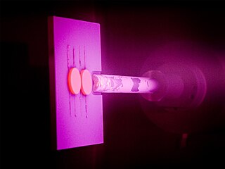
Plasma-enhanced chemical vapor deposition (PECVD) is a chemical vapor deposition process used to deposit thin films from a gas state (vapor) to a solid state on a substrate. Chemical reactions are involved in the process, which occur after creation of a plasma of the reacting gases. The plasma is generally created by radio frequency (RF) alternating current (AC) frequency or direct current (DC) discharge between two electrodes, the space between which is filled with the reacting gases.

Evaporation is a common method of thin-film deposition. The source material is evaporated in a vacuum. The vacuum allows vapor particles to travel directly to the target object (substrate), where they condense back to a solid state. Evaporation is used in microfabrication, and to make macro-scale products such as metallized plastic film.

Sputter deposition is a physical vapor deposition (PVD) method of thin film deposition by the phenomenon of sputtering. This involves ejecting material from a "target" that is a source onto a "substrate" such as a silicon wafer.
Electron-beam additive manufacturing, or electron-beam melting (EBM) is a type of additive manufacturing, or 3D printing, for metal parts. The raw material is placed under a vacuum and fused together from heating by an electron beam. This technique is distinct from selective laser sintering as the raw material fuses have completely melted. Selective Electron Beam Melting (SEBM) emerged as a powder bed-based additive manufacturing (AM) technology and was brought to market in 1997 by Arcam AB Corporation headquartered in Sweden.
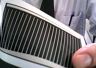
A copper indium gallium selenide solar cell is a thin-film solar cell used to convert sunlight into electric power. It is manufactured by depositing a thin layer of copper indium gallium selenide solid solution on glass or plastic backing, along with electrodes on the front and back to collect current. Because the material has a high absorption coefficient and strongly absorbs sunlight, a much thinner film is required than of other semiconductor materials.

Electromagnetically-enhanced Physical Vapor Deposition (EPVD) is coating technique developed by Paradigm Shift Technologies, Inc. which uses electromagnetic fields to improve traditional physical vapor deposition, particularly in high-stress applications like gun barrel coatings.