
The metal–oxide–semiconductor field-effect transistor is a type of field-effect transistor (FET), most commonly fabricated by the controlled oxidation of silicon. It has an insulated gate, the voltage of which determines the conductivity of the device. This ability to change conductivity with the amount of applied voltage can be used for amplifying or switching electronic signals. The term metal–insulator–semiconductor field-effect transistor (MISFET) is almost synonymous with MOSFET. Another near-synonym is insulated-gate field-effect transistor (IGFET).

Complementary metal–oxide–semiconductor is a type of metal–oxide–semiconductor field-effect transistor (MOSFET) fabrication process that uses complementary and symmetrical pairs of p-type and n-type MOSFETs for logic functions. CMOS technology is used for constructing integrated circuit (IC) chips, including microprocessors, microcontrollers, memory chips, and other digital logic circuits. CMOS technology is also used for analog circuits such as image sensors, data converters, RF circuits, and highly integrated transceivers for many types of communication.
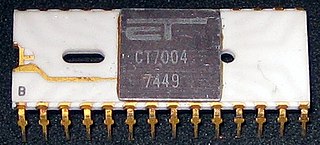
A programmable read-only memory (PROM) is a form of digital memory where the contents can be changed once after manufacture of the device. The data is then permanent and cannot be changed. It is one type of read-only memory (ROM). PROMs are used in digital electronic devices to store permanent data, usually low level programs such as firmware or microcode. The key difference from a standard ROM is that the data is written into a ROM during manufacture, while with a PROM the data is programmed into them after manufacture. Thus, ROMs tend to be used only for large production runs with well-verified data. PROMs may be used where the volume required does not make a factory-programmed ROM economical, or during development of a system that may ultimately be converted to ROMs in a mass produced version.

Flash memory is an electronic non-volatile computer memory storage medium that can be electrically erased and reprogrammed. The two main types of flash memory, NOR flash and NAND flash, are named for the NOR and NAND logic gates. Both use the same cell design, consisting of floating gate MOSFETs. They differ at the circuit level depending on whether the state of the bit line or word lines is pulled high or low: in NAND flash, the relationship between the bit line and the word lines resembles a NAND gate; in NOR flash, it resembles a NOR gate.

EEPROM or E2PROM (electrically erasable programmable read-only memory) is a type of non-volatile memory. It is used in computers, usually integrated in microcontrollers such as smart cards and remote keyless systems, or as a separate chip device, to store relatively small amounts of data by allowing individual bytes to be erased and reprogrammed.

A programmable logic device (PLD) is an electronic component used to build reconfigurable digital circuits. Unlike digital logic constructed using discrete logic gates with fixed functions, the function of a PLD is undefined at the time of manufacture. Before the PLD can be used in a circuit it must be programmed to implement the desired function. Compared to fixed logic devices, programmable logic devices simplify the design of complex logic and may offer superior performance. Unlike for microprocessors, programming a PLD changes the connections made between the gates in the device.

An EPROM, or erasable programmable read-only memory, is a type of programmable read-only memory (PROM) chip that retains its data when its power supply is switched off. Computer memory that can retrieve stored data after a power supply has been turned off and back on is called non-volatile. It is an array of floating-gate transistors individually programmed by an electronic device that supplies higher voltages than those normally used in digital circuits. Once programmed, an EPROM can be erased by exposing it to strong ultraviolet (UV) light source. EPROMs are easily recognizable by the transparent fused quartz window on the top of the package, through which the silicon chip is visible, and which permits exposure to ultraviolet light during erasing.

Programmable Array Logic (PAL) is a family of programmable logic device semiconductors used to implement logic functions in digital circuits that was introduced by Monolithic Memories, Inc. (MMI) in March 1978. MMI obtained a registered trademark on the term PAL for use in "Programmable Semiconductor Logic Circuits". The trademark is currently held by Lattice Semiconductor.

In electronics and electrical engineering, a fuse is an electrical safety device that operates to provide overcurrent protection of an electrical circuit. Its essential component is a metal wire or strip that melts when too much current flows through it, thereby stopping or interrupting the current. It is a sacrificial device; once a fuse has operated, it is an open circuit, and must be replaced or rewired, depending on its type.
An antifuse is an electrical device that performs the opposite function to a fuse. Whereas a fuse starts with a low resistance and is designed to permanently break or open an electrically conductive path, an antifuse starts with a high resistance--an open circuit--and programming it converts it into a permanent electrically conductive path. This technology has many applications. Antifuses are best known for their use in mini-light style low-voltage Christmas tree lights.
Non-volatile memory (NVM) or non-volatile storage is a type of computer memory that can retain stored information even after power is removed. In contrast, volatile memory needs constant power in order to retain data.
Charge trap flash (CTF) is a semiconductor memory technology used in creating non-volatile NOR and NAND flash memory. It is a type of floating-gate MOSFET memory technology, but differs from the conventional floating-gate technology in that it uses a silicon nitride film to store electrons rather than the doped polycrystalline silicon typical of a floating-gate structure. This approach allows memory manufacturers to reduce manufacturing costs five ways:
- Fewer process steps are required to form a charge storage node
- Smaller process geometries can be used
- Multiple bits can be stored on a single flash memory cell
- Improved reliability
- Higher yield since the charge trap is less susceptible to point defects in the tunnel oxide layer
SONOS, short for "silicon–oxide–nitride–oxide–silicon", more precisely, "polycrystalline silicon"—"silicon dioxide"—"silicon nitride"—"silicon dioxide"—"silicon", is a cross sectional structure of MOSFET (metal–oxide–semiconductor field-effect transistor), realized by P.C.Y. Chen of Fairchild Camera and Instrument in 1977. This structure is often used for non-volatile memories, such as EEPROM and flash memories. It is sometimes used for TFT LCD displays. It is one of CTF (charge trap flash) variants. It is distinguished from traditional non-volatile memory structures by the use of silicon nitride (Si3N4 or Si9N10) instead of "polysilicon-based FG (floating-gate)" for the charge storage material. A further variant is "SHINOS" ("silicon"—"hi-k"—"nitride"—"oxide"—"silicon"), which is substituted top oxide layer with high-κ material. Another advanced variant is "MONOS" ("metal–oxide–nitride–oxide–silicon"). Companies offering SONOS-based products include Cypress Semiconductor, Macronix, Toshiba, United Microelectronics Corporation and Floadia.
In semiconductor electronics fabrication technology, a self-aligned gate is a transistor manufacturing approach whereby the gate electrode of a MOSFET is used as a mask for the doping of the source and drain regions. This technique ensures that the gate is naturally and precisely aligned to the edges of the source and drain.
Resistive random-access memory is a type of non-volatile (NV) random-access (RAM) computer memory that works by changing the resistance across a dielectric solid-state material, often referred to as a memristor. One major advantage of ReRAM over other NVRAM technologies is the ability to scale below 10nm.
PMOS or pMOS logic is a family of digital circuits based on p-channel, enhancement mode metal–oxide–semiconductor field-effect transistors (MOSFETs). In the late 1960s and early 1970s, PMOS logic was the dominant semiconductor technology for large-scale integrated circuits before being superseded by NMOS and CMOS devices.

Read-only memory (ROM) is a type of non-volatile memory used in computers and other electronic devices. Data stored in ROM cannot be electronically modified after the manufacture of the memory device. Read-only memory is useful for storing software that is rarely changed during the life of the system, also known as firmware. Software applications for programmable devices can be distributed as plug-in cartridges containing ROM.
Electronic components have a wide range of failure modes. These can be classified in various ways, such as by time or cause. Failures can be caused by excess temperature, excess current or voltage, ionizing radiation, mechanical shock, stress or impact, and many other causes. In semiconductor devices, problems in the device package may cause failures due to contamination, mechanical stress of the device, or open or short circuits.
A nanoelectromechanical (NEM) relay is an electrically actuatedswitch that is built on the nanometer scale using semiconductor fabrication techniques. They are designed to operate in replacement of, or in conjunction with, traditional semiconductor logic. While the mechanical nature of NEM relays makes them switch much slower than solid-state relays, they have many advantageous properties, such as zero current leakage and low power consumption, which make them potentially useful in next generation computing.
Electrochemical Random-Access Memory (ECRAM) is a type of non-volatile memory (NVM) with multiple levels per cell (MLC) designed for deep learning analog acceleration. An ECRAM cell is a three-terminal device composed of a conductive channel, an insulating electrolyte, an ionic reservoir, and metal contacts. The resistance of the channel is modulated by ionic exchange at the interface between the channel and the electrolyte upon application of an electric field. The charge-transfer process allows both for state retention in the absence of applied power, and for programming of multiple distinct levels, both differentiating ECRAM operation from that of a field-effect transistor (FET). The write operation is deterministic and can result in symmetrical potentiation and depression, making ECRAM arrays attractive for acting as artificial synaptic weights in physical implementations of artificial neural networks (ANN). The technological challenges include open circuit potential (OCP) and semiconductor foundry compatibility associated with energy materials. Universities, government laboratories, and corporate research teams have contributed to the development of ECRAM for analog computing. Notably, Sandia National Laboratories designed a lithium-based cell inspired by solid-state battery materials, Stanford University built an organic proton-based cell, and International Business Machines (IBM) demonstrated in-memory selector-free parallel programming for a logistic regression task in an array of metal-oxide ECRAM designed for insertion in the back end of line (BEOL). In 2022, researchers at Massachusetts Institute of Technology built an inorganic, CMOS-compatible protonic technology that achieved near-ideal modulation characteristics using nanosecond fast pulses