A semiconductor is a material that has an electrical conductivity value falling between that of a conductor, such as copper, and an insulator, such as glass. Its resistivity generally falls as its temperature rises; metals behave in the opposite way. In many cases their conducting properties may be altered in useful ways by introducing impurities ("doping") into the crystal structure. When two differently doped regions exist in the same crystal, a semiconductor junction is created. The behavior of charge carriers, which include electrons, ions, and electron holes, at these junctions is the basis of diodes, transistors, and most modern electronics. Some examples of semiconductors are silicon, germanium, gallium arsenide, and elements near the so-called "metalloid staircase" on the periodic table. After silicon, gallium arsenide is the second-most common semiconductor and is used in laser diodes, solar cells, microwave-frequency integrated circuits, and others. Silicon is a critical element for fabricating most electronic circuits.

A transistor is a semiconductor device used to amplify or switch electrical signals and power. It is one of the basic building blocks of modern electronics. It is composed of semiconductor material, usually with at least three terminals for connection to an electronic circuit. A voltage or current applied to one pair of the transistor's terminals controls the current through another pair of terminals. Because the controlled (output) power can be higher than the controlling (input) power, a transistor can amplify a signal. Some transistors are packaged individually, but many more in miniature form are found embedded in integrated circuits. Because transistors are the key active components in practically all modern electronics, many people consider them one of the 20th century's greatest inventions.

A semiconductor device is an electronic component that relies on the electronic properties of a semiconductor material for its function. Its conductivity lies between conductors and insulators. Semiconductor devices have replaced vacuum tubes in most applications. They conduct electric current in the solid state, rather than as free electrons across a vacuum or as free electrons and ions through an ionized gas.

The metal–oxide–semiconductor field-effect transistor is a type of field-effect transistor (FET), most commonly fabricated by the controlled oxidation of silicon. It has an insulated gate, the voltage of which determines the conductivity of the device. This ability to change conductivity with the amount of applied voltage can be used for amplifying or switching electronic signals. The term metal–insulator–semiconductor field-effect transistor (MISFET) is almost synonymous with MOSFET. Another near-synonym is insulated-gate field-effect transistor (IGFET).
In solid-state physics, the electron mobility characterises how quickly an electron can move through a metal or semiconductor when pulled by an electric field. There is an analogous quantity for holes, called hole mobility. The term carrier mobility refers in general to both electron and hole mobility.

A high-electron-mobility transistor, also known as heterostructure FET (HFET) or modulation-doped FET (MODFET), is a field-effect transistor incorporating a junction between two materials with different band gaps as the channel instead of a doped region. A commonly used material combination is GaAs with AlGaAs, though there is wide variation, dependent on the application of the device. Devices incorporating more indium generally show better high-frequency performance, while in recent years, gallium nitride HEMTs have attracted attention due to their high-power performance. Like other FETs, HEMTs are used in integrated circuits as digital on-off switches. FETs can also be used as amplifiers for large amounts of current using a small voltage as a control signal. Both of these uses are made possible by the FET’s unique current–voltage characteristics. HEMT transistors are able to operate at higher frequencies than ordinary transistors, up to millimeter wave frequencies, and are used in high-frequency products such as cell phones, satellite television receivers, voltage converters, and radar equipment. They are widely used in satellite receivers, in low power amplifiers and in the defense industry.

In semiconductor production, doping is the intentional introduction of impurities into an intrinsic (undoped) semiconductor for the purpose of modulating its electrical, optical and structural properties. The doped material is referred to as an extrinsic semiconductor.

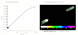
For power semiconductor devices, the safe operating area (SOA) is defined as the voltage and current conditions over which the device can be expected to operate without self-damage.
The threshold voltage, commonly abbreviated as Vth or VGS(th), of a field-effect transistor (FET) is the minimum gate-to-source voltage (VGS) that is needed to create a conducting path between the source and drain terminals. It is an important scaling factor to maintain power efficiency.
In the semiconductor industry, the term high-κ dielectric refers to a material with a high dielectric constant, as compared to silicon dioxide. High-κ dielectrics are used in semiconductor manufacturing processes where they are usually used to replace a silicon dioxide gate dielectric or another dielectric layer of a device. The implementation of high-κ gate dielectrics is one of several strategies developed to allow further miniaturization of microelectronic components, colloquially referred to as extending Moore's Law. Sometimes these materials are called "high-k", instead of "high-κ".
In semiconductor electronics fabrication technology, a self-aligned gate is a transistor manufacturing approach whereby the gate electrode of a MOSFET is used as a mask for the doping of the source and drain regions. This technique ensures that the gate is naturally and precisely aligned to the edges of the source and drain.
Multi-threshold CMOS (MTCMOS) is a variation of CMOS chip technology which has transistors with multiple threshold voltages (Vth) in order to optimize delay or power. The Vth of a MOSFET is the gate voltage where an inversion layer forms at the interface between the insulating layer (oxide) and the substrate (body) of the transistor. Low Vth devices switch faster, and are therefore useful on critical delay paths to minimize clock periods. The penalty is that low Vth devices have substantially higher static leakage power. High Vth devices are used on non-critical paths to reduce static leakage power without incurring a delay penalty. Typical high Vth devices reduce static leakage by 10 times compared with low Vth devices.
An extrinsic semiconductor is one that has been doped; during manufacture of the semiconductor crystal a trace element or chemical called a doping agent has been incorporated chemically into the crystal, for the purpose of giving it different electrical properties than the pure semiconductor crystal, which is called an intrinsic semiconductor. In an extrinsic semiconductor it is these foreign dopant atoms in the crystal lattice that mainly provide the charge carriers which carry electric current through the crystal. The doping agents used are of two types, resulting in two types of extrinsic semiconductor. An electron donor dopant is an atom which, when incorporated in the crystal, releases a mobile conduction electron into the crystal lattice. An extrinsic semiconductor that has been doped with electron donor atoms is called an n-type semiconductor, because the majority of charge carriers in the crystal are negative electrons. An electron acceptor dopant is an atom which accepts an electron from the lattice, creating a vacancy where an electron should be called a hole which can move through the crystal like a positively charged particle. An extrinsic semiconductor which has been doped with electron acceptor atoms is called a p-type semiconductor, because the majority of charge carriers in the crystal are positive holes.

A metal gate, in the context of a lateral metal–oxide–semiconductor (MOS) stack, is the gate electrode separated by an oxide from the transistor's channel – the gate material is made from a metal. In most MOS transistors since about the mid-1970s, the "M" for metal has been replaced by polysilicon, but the name remained.
For electronic semiconductor devices, a native transistor is a variety of the MOS field-effect transistor that is intermediate between enhancement and depletion modes. Most common is the n-channel native transistor.
Process variation is the naturally occurring variation in the attributes of transistors when integrated circuits are fabricated. The amount of process variation becomes particularly pronounced at smaller process nodes (<65 nm) as the variation becomes a larger percentage of the full length or width of the device and as feature sizes approach the fundamental dimensions such as the size of atoms and the wavelength of usable light for patterning lithography masks.
Polysilicon depletion effect is the phenomenon in which unwanted variation of threshold voltage of the MOSFET devices using polysilicon as gate material is observed, leading to unpredicted behavior of the electronic circuit. Because of this variation High-k Dielectric Metal Gates (HKMG) were introduced to solve the issue.

In physics, the field effect refers to the modulation of the electrical conductivity of a material by the application of an external electric field.

The field-effect transistor (FET) is a type of transistor that uses an electric field to control the flow of current in a semiconductor. It comes in two types: junction FET (JFET) and metal-oxide-semiconductor FET (MOSFET). FETs have three terminals: source, gate, and drain. FETs control the flow of current by the application of a voltage to the gate, which in turn alters the conductivity between the drain and source.
Transistor aging is the process of silicon transistors developing flaws over time as they are used, degrading performance and reliability, and eventually failing altogether. Despite the name, similar mechanisms may affect transistors made of any kind of semiconductor. Manufacturers compensate for this by running chips at slower speeds than they are initially capable of (underclocking).