In optics, aberration is a property of optical systems, such as lenses, that causes light to be spread out over some region of space rather than focused to a point. Aberrations cause the image formed by a lens to be blurred or distorted, with the nature of the distortion depending on the type of aberration. Aberration can be defined as a departure of the performance of an optical system from the predictions of paraxial optics. In an imaging system, it occurs when light from one point of an object does not converge into a single point after transmission through the system. Aberrations occur because the simple paraxial theory is not a completely accurate model of the effect of an optical system on light, rather than due to flaws in the optical elements.

A microscope is a laboratory instrument used to examine objects that are too small to be seen by the naked eye. Microscopy is the science of investigating small objects and structures using a microscope. Microscopic means being invisible to the eye unless aided by a microscope.

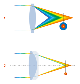
In optics, chromatic aberration (CA), also called chromatic distortion and spherochromatism, is a failure of a lens to focus all colors to the same point. It is caused by dispersion: the refractive index of the lens elements varies with the wavelength of light. The refractive index of most transparent materials decreases with increasing wavelength. Since the focal length of a lens depends on the refractive index, this variation in refractive index affects focusing. Chromatic aberration manifests itself as "fringes" of color along boundaries that separate dark and bright parts of the image.

Transmission electron microscopy (TEM) is a microscopy technique in which a beam of electrons is transmitted through a specimen to form an image. The specimen is most often an ultrathin section less than 100 nm thick or a suspension on a grid. An image is formed from the interaction of the electrons with the sample as the beam is transmitted through the specimen. The image is then magnified and focused onto an imaging device, such as a fluorescent screen, a layer of photographic film, or a sensor such as a scintillator attached to a charge-coupled device.

The resolution of an optical imaging system – a microscope, telescope, or camera – can be limited by factors such as imperfections in the lenses or misalignment. However, there is a principal limit to the resolution of any optical system, due to the physics of diffraction. An optical system with resolution performance at the instrument's theoretical limit is said to be diffraction-limited.

In optical engineering, the objective is the optical element that gathers light from the object being observed and focuses the light rays to produce a real image. Objectives can be a single lens or mirror, or combinations of several optical elements. They are used in microscopes, binoculars, telescopes, cameras, slide projectors, CD players and many other optical instruments. Objectives are also called object lenses, object glasses, or objective glasses.
Photoemission electron microscopy is a type of electron microscopy that utilizes local variations in electron emission to generate image contrast. The excitation is usually produced by ultraviolet light, synchrotron radiation or X-ray sources. PEEM measures the coefficient indirectly by collecting the emitted secondary electrons generated in the electron cascade that follows the creation of the primary core hole in the absorption process. PEEM is a surface sensitive technique because the emitted electrons originate from a shallow layer. In physics, this technique is referred to as PEEM, which goes together naturally with low-energy electron diffraction (LEED), and low-energy electron microscopy (LEEM). In biology, it is called photoelectron microscopy (PEM), which fits with photoelectron spectroscopy (PES), transmission electron microscopy (TEM), and scanning electron microscopy (SEM).
An electrostatic lens is a device that assists in the transport of charged particles. For instance, it can guide electrons emitted from a sample to an electron analyzer, analogous to the way an optical lens assists in the transport of light in an optical instrument. Systems of electrostatic lenses can be designed in the same way as optical lenses, so electrostatic lenses easily magnify or converge the electron trajectories. An electrostatic lens can also be used to focus an ion beam, for example to make a microbeam for irradiating individual cells.

Transmission Electron Aberration-Corrected Microscope (TEAM) is a collaborative research project between four US laboratories and two companies. The project's main activity is design and application of a transmission electron microscope (TEM) with a spatial resolution below 0.05 nanometers, which is roughly half the size of an atom of hydrogen.

Electron optics is a mathematical framework for the calculation of electron trajectories in the presence of electromagnetic fields. The term optics is used because magnetic and electrostatic lenses act upon a charged particle beam similarly to optical lenses upon a light beam.
An electron spectrometer is a device used to perform different forms of electron spectroscopy and electron microscopy. This requires analyzing the energy of an incoming beam of electrons. Most electron spectrometers use a hemispherical electron energy analyzer in which the beam of electrons is bent with electric or magnetic fields. Higher energy electrons will be bent less by the beam, this produces a spatially distributed range of energies.
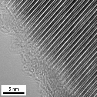
High-resolution transmission electron microscopy is an imaging mode of specialized transmission electron microscopes that allows for direct imaging of the atomic structure of samples. It is a powerful tool to study properties of materials on the atomic scale, such as semiconductors, metals, nanoparticles and sp2-bonded carbon. While this term is often also used to refer to high resolution scanning transmission electron microscopy, mostly in high angle annular dark field mode, this article describes mainly the imaging of an object by recording the two-dimensional spatial wave amplitude distribution in the image plane, similar to a "classic" light microscope. For disambiguation, the technique is also often referred to as phase contrast transmission electron microscopy, although this term is less appropriate. At present, the highest point resolution realised in high resolution transmission electron microscopy is around 0.5 ångströms (0.050 nm). At these small scales, individual atoms of a crystal and defects can be resolved. For 3-dimensional crystals, it is necessary to combine several views, taken from different angles, into a 3D map. This technique is called electron tomography.

Otto Scherzer was a German theoretical physicist who made contributions to electron microscopy.
A magnetic lens is a device for the focusing or deflection of moving charged particles, such as electrons or ions, by use of the magnetic Lorentz force. Its strength can often be varied by usage of electromagnets.
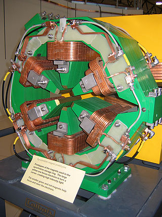
A sextupole magnet consist of six magnetic poles set out in an arrangement of alternating north and south poles arranged around an axis. They are used in particle accelerators for the control of chromatic aberrations and for damping the head tail instability. Two sets of sextupole magnets are used in transmission electron microscopes to correct for spherical aberration.

The contrast transfer function (CTF) mathematically describes how aberrations in a transmission electron microscope (TEM) modify the image of a sample. This contrast transfer function (CTF) sets the resolution of high-resolution transmission electron microscopy (HRTEM), also known as phase contrast TEM.
The Ernst Ruska-Centre for Microscopy and Spectroscopy with Electrons (ER-C) is an institute located on the campus of Forschungszentrum Jülich belonging to the Helmholtz Association of German Research Centres. It comprises three divisions: ER-C-1 “Physics of Nanoscale systems”, ER-C-2 “Materials Science and Technology” and ER-C-3 “Structural Biology”.

A condenser is an optical lens which renders a divergent beam from a point source into a parallel or converging beam to illuminate an object.

Harald Rose is a German physicist.
A stigmator is a component of electron microscopes that reduces astigmatism of the beam by imposing a weak electric or magnetic quadrupole field on the electron beam.