An avalanche photodiode (APD) is a highly sensitive type of photodiode, which in general are semiconductor diodes that convert light into electricity via interband excitation coupled with impact ionization. APDs use materials and a structure optimised for operating with high reverse bias, approaching the reverse breakdown voltage, such that charge carriers generated by the photoelectric effect are multiplied by an avalanche breakdown; thus they can be used to detect relatively small amounts of light.

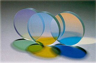
In the field of optics, transparency is the physical property of allowing light to pass through the material without appreciable scattering of light. On a macroscopic scale, the photons can be said to follow Snell's law. Translucency allows light to pass through but does not necessarily follow Snell's law; the photons can be scattered at either of the two interfaces, or internally, where there is a change in the index of refraction. In other words, a translucent material is made up of components with different indices of refraction. A transparent material is made up of components with a uniform index of refraction. Transparent materials appear clear, with the overall appearance of one color, or any combination leading up to a brilliant spectrum of every color. The opposite property of translucency is opacity. Other categories of visual appearance, related to the perception of regular or diffuse reflection and transmission of light, have been organized under the concept of cesia in an order system with three variables, including transparency, translucency and opacity among the involved aspects.

A photonic crystal is an optical nanostructure in which the refractive index changes periodically. This affects the propagation of light in the same way that the structure of natural crystals gives rise to X-ray diffraction and that the atomic lattices of semiconductors affect their conductivity of electrons. Photonic crystals occur in nature in the form of structural coloration and animal reflectors, and, as artificially produced, promise to be useful in a range of applications.

Indium phosphide (InP) is a binary semiconductor composed of indium and phosphorus. It has a face-centered cubic ("zincblende") crystal structure, identical to that of GaAs and most of the III-V semiconductors.

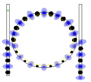
An optical ring resonator is a set of waveguides in which at least one is a closed loop coupled to some sort of light input and output. The concepts behind optical ring resonators are the same as those behind whispering galleries except that they use light and obey the properties behind constructive interference and total internal reflection. When light of the resonant wavelength is passed through the loop from the input waveguide, the light builds up in intensity over multiple round-trips owing to constructive interference and is output to the output bus waveguide which serves as a detector waveguide. Because only a select few wavelengths will be at resonance within the loop, the optical ring resonator functions as a filter. Additionally, as implied earlier, two or more ring waveguides can be coupled to each other to form an add/drop optical filter.
Quantum-cascade lasers (QCLs) are semiconductor lasers that emit in the mid- to far-infrared portion of the electromagnetic spectrum and were first demonstrated by Jérôme Faist, Federico Capasso, Deborah Sivco, Carlo Sirtori, Albert Hutchinson, and Alfred Cho at Bell Laboratories in 1994.

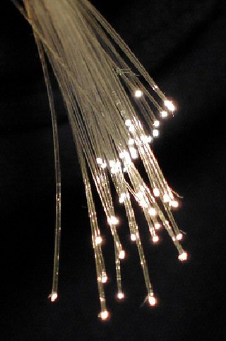
An optical fiber, or optical fibre, is a flexible glass or plastic fiber that can transmit light from one end to the other. Such fibers find wide usage in fiber-optic communications, where they permit transmission over longer distances and at higher bandwidths than electrical cables. Fibers are used instead of metal wires because signals travel along them with less loss and are immune to electromagnetic interference. Fibers are also used for illumination and imaging, and are often wrapped in bundles so they may be used to carry light into, or images out of confined spaces, as in the case of a fiberscope. Specially designed fibers are also used for a variety of other applications, such as fiber optic sensors and fiber lasers.
An optical waveguide is a physical structure that guides electromagnetic waves in the optical spectrum. Common types of optical waveguides include optical fiber waveguides, transparent dielectric waveguides made of plastic and glass, liquid light guides, and liquid waveguides.
A photonic integrated circuit (PIC) or integrated optical circuit is a microchip containing two or more photonic components that form a functioning circuit. This technology detects, generates, transports, and processes light. Photonic integrated circuits use photons as opposed to electrons that are used by electronic integrated circuits. The major difference between the two is that a photonic integrated circuit provides functions for information signals imposed on optical wavelengths typically in the visible spectrum or near-infrared (850–1650 nm).
A hybrid silicon laser is a semiconductor laser fabricated from both silicon and group III-V semiconductor materials. The hybrid silicon laser was developed to address the lack of a silicon laser to enable fabrication of low-cost, mass-producible silicon optical devices. The hybrid approach takes advantage of the light-emitting properties of III-V semiconductor materials combined with the process maturity of silicon to fabricate electrically driven lasers on a silicon wafer that can be integrated with other silicon photonic devices.

Silicon photonics is the study and application of photonic systems which use silicon as an optical medium. The silicon is usually patterned with sub-micrometre precision, into microphotonic components. These operate in the infrared, most commonly at the 1.55 micrometre wavelength used by most fiber optic telecommunication systems. The silicon typically lies on top of a layer of silica in what is known as silicon on insulator (SOI).

Charles H. Henry was an American physicist. He was born in Chicago, Illinois. He received an M.S. degree in physics in 1959 from the University of Chicago, and a Ph.D. degree in physics in 1965 from the University of Illinois, under the direction of Charlie Slichter. In March 2008, he was featured in an article in the Physics Illinois News, a publication of the Physics Department of the University of Illinois.

A slot-waveguide is an optical waveguide that guides strongly confined light in a subwavelength-scale low refractive index region by total internal reflection.
The quantum-confined Stark effect (QCSE) describes the effect of an external electric field upon the light absorption spectrum or emission spectrum of a quantum well (QW). In the absence of an external electric field, electrons and holes within the quantum well may only occupy states within a discrete set of energy subbands. Only a discrete set of frequencies of light may be absorbed or emitted by the system. When an external electric field is applied, the electron states shift to lower energies, while the hole states shift to higher energies. This reduces the permitted light absorption or emission frequencies. Additionally, the external electric field shifts electrons and holes to opposite sides of the well, decreasing the overlap integral, which in turn reduces the recombination efficiency of the system. The spatial separation between the electrons and holes is limited by the presence of the potential barriers around the quantum well, meaning that excitons are able to exist in the system even under the influence of an electric field. The quantum-confined Stark effect is used in QCSE optical modulators, which allow optical communications signals to be switched on and off rapidly.
An optical modulator is an optical device which is used to modulate a beam of light with a perturbation device. It is a kind of transmitter to convert information to optical binary signal through optical fiber or transmission medium of optical frequency in fiber optic communication. There are several methods to manipulate this device depending on the parameter of a light beam like amplitude modulator (majority), phase modulator, polarization modulator etc. The easiest way to obtain modulation is modulation of intensity of a light by the current driving the light source. This sort of modulation is called direct modulation, as opposed to the external modulation performed by a light modulator. For this reason, light modulators are called external light modulators. According to manipulation of the properties of material modulators are divided into two groups, absorptive modulators and refractive modulators. Absorption coefficient can be manipulated by Franz-Keldysh effect, Quantum-Confined Stark Effect, excitonic absorption, or changes of free carrier concentration. Usually, if several such effects appear together, the modulator is called electro-absorptive modulator. Refractive modulators most often make use of electro-optic effect, other modulators are made with acousto-optic effect, magneto-optic effect such as Faraday and Cotton-Mouton effects. The other case of modulators is spatial light modulator (SLM) which is modified two dimensional distribution of amplitude & phase of an optical wave.
A plasmonic-enhanced solar cell, commonly referred to simply as plasmonic solar cell, is a type of solar cell that converts light into electricity with the assistance of plasmons, but where the photovoltaic effect occurs in another material.
Two-photon photovoltaic effect is an energy collection method based on two-photon absorption (TPA). The TPP effect can be thought of as the nonlinear equivalent of the traditional photovoltaic effect involving high optical intensities. This effect occurs when two photons are absorbed at the same time resulting in an electron-hole pair.
Integrated quantum photonics, uses photonic integrated circuits to control photonic quantum states for applications in quantum technologies. As such, integrated quantum photonics provides a promising approach to the miniaturisation and scaling up of optical quantum circuits. The major application of integrated quantum photonics is Quantum technology:, for example quantum computing, quantum communication, quantum simulation, quantum walks and quantum metrology.

Prof. R K Sinha is the Vice Chancellor of Gautam Buddha University, Greater Noida, Gautam Budh Nagar under Uttar Pradesh Government since January 2022. He was the Director of the CSIR-Central Scientific Instruments Organisation (CSIR-CSIO) Sector-30C, Chandigarh-160 030, India. He has been a Professor - Applied Physics, Dean-Academic [UG] & Chief Coordinator: TIFAC-Center of Relevance and Excellence in Fiber Optics and Optical Communication, Mission REACH Program, Technology Vision-2020, Govt. of India Delhi Technological University Bawana Road, Delhi-110042, India.
The Urbach Energy, or Urbach Edge, is a parameter typically denoted , with dimensions of energy, used to quantify energetic disorder in the band edges of a semiconductor. It is evaluated by fitting the absorption coefficient as a function of energy to an exponential function. It is often used to describe electron transport in structurally disordered semiconductors such as hydrogenated amorphous silicon.
