The Kirkendall effect is the motion of the interface between two metals that occurs as a consequence of the difference in diffusion rates of the metal atoms. The effect can be observed for example by placing insoluble markers at the interface between a pure metal and an alloy containing that metal, and heating to a temperature where atomic diffusion is possible; the boundary will move relative to the markers.

A printed circuit board (PCB) mechanically supports and electrically connects electronic components or electrical components using conductive tracks, pads and other features etched from one or more sheet layers of copper laminated onto and/or between sheet layers of a non-conductive substrate. Components are generally soldered onto the PCB to both electrically connect and mechanically fasten them to it.
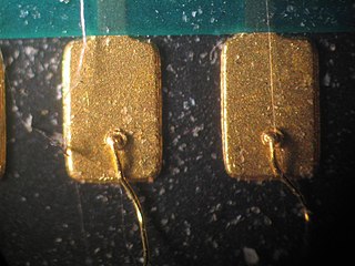
Wire bonding is the method of making interconnections (ATJ) between an integrated circuit (IC) or other semiconductor device and its packaging during semiconductor device fabrication. Although less common, wire bonding can be used to connect an IC to other electronics or to connect from one printed circuit board (PCB) to another. Wire bonding is generally considered the most cost-effective and flexible interconnect technology and is used to assemble the vast majority of semiconductor packages. Wire bonding can be used at frequencies above 100 GHz.
A fracture is the separation of an object or material into two or more pieces under the action of stress. The fracture of a solid usually occurs due to the development of certain displacement discontinuity surfaces within the solid. If a displacement develops perpendicular to the surface of displacement, it is called a normal tensile crack or simply a crack; if a displacement develops tangentially to the surface of displacement, it is called a shear crack, slip band, or dislocation.

Electromigration is the transport of material caused by the gradual movement of the ions in a conductor due to the momentum transfer between conducting electrons and diffusing metal atoms. The effect is important in applications where high direct current densities are used, such as in microelectronics and related structures. As the structure size in electronics such as integrated circuits (ICs) decreases, the practical significance of this effect increases.
In materials science, creep is the tendency of a solid material to move slowly or deform permanently under the influence of mechanical stresses. It can occur as a result of long-term exposure to high levels of stress that are still below the yield strength of the material. Creep is more severe in materials that are subjected to heat for long periods, and generally increases as they near their melting point.

Metal whiskering is a phenomenon which occurs in electrical devices when metals form long whisker-like projections over time. Tin whiskers were noticed and documented in the vacuum tube era of electronics early in the 20th century in equipment that used pure, or almost pure, tin solder in their production. It was noticed that small metal hairs or tendrils grew between metal solder pads causing short circuits. Metal whiskers form in the presence of compressive stress. Zinc, cadmium, and even lead whiskers have been documented. Many techniques are used to mitigate the problem including changes to the annealing process, addition of elements like copper and nickel, and the inclusion of conformal coatings. Traditionally, lead was added to slow down whisker growth in tin-based solders.
A power cable is an electrical cable, an assembly of one or more electrical conductors, usually held together with an overall sheath. The assembly is used for transmission of electrical power. Power cables may be installed as permanent wiring within buildings, buried in the ground, run overhead, or exposed.

A reactor pressure vessel (RPV) in a nuclear power plant is the pressure vessel containing the nuclear reactor coolant, core shroud, and the reactor core.
Annealing, in metallurgy and materials science, is a heat treatment that alters the physical and sometimes chemical properties of a material to increase its ductility and reduce its hardness, making it more workable. It involves heating a material above its recrystallization temperature, maintaining a suitable temperature for a suitable amount of time, and then cooling.
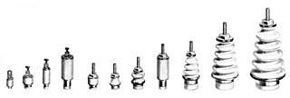
In electric power, a bushing is an insulated device that allows an electrical conductor to pass safely through a grounded conducting barrier such as the case of a transformer or circuit breaker. Bushings are typically made from porcelain; though other insulating materials are also possible, generally porcelain is used.
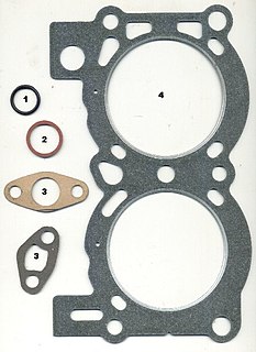
A head gasket is a gasket that sits between the engine block and cylinder head(s) in an internal combustion engine.

Flat no-leads packages such as quad-flat no-leads (QFN) and dual-flat no-leads (DFN) physically and electrically connect integrated circuits to printed circuit boards. Flat no-leads, also known as micro leadframe (MLF) and SON, is a surface-mount technology, one of several package technologies that connect ICs to the surfaces of PCBs without through-holes. Flat no-lead is a near chip scale plastic encapsulated package made with a planar copper lead frame substrate. Perimeter lands on the package bottom provide electrical connections to the PCB. Flat no-lead packages include an exposed thermal pad to improve heat transfer out of the IC. Heat transfer can be further facilitated by metal vias in the thermal pad. The QFN package is similar to the quad-flat package (QFP), and a ball grid array (BGA).
Diffusion creep refers to the deformation of crystalline solids by the diffusion of vacancies through their crystal lattice. Diffusion creep results in plastic deformation rather than brittle failure of the material.
Electronic packaging is the design and production of enclosures for electronic devices ranging from individual semiconductor devices up to complete systems such as a mainframe computer. Packaging of an electronic system must consider protection from mechanical damage, cooling, radio frequency noise emission and electrostatic discharge. Product safety standards may dictate particular features of a consumer product, for example, external case temperature or grounding of exposed metal parts. Prototypes and industrial equipment made in small quantities may use standardized commercially available enclosures such as card cages or prefabricated boxes. Mass-market consumer devices may have highly specialized packaging to increase consumer appeal. Electronic packaging is a major discipline within the field of mechanical engineering.
In structural geology, metallurgy and materials science, deformation mechanisms refer to the various mechanisms at the grain scale that are responsible for accommodating large plastic strains in rocks, metals and other materials.
Microvias are used as the interconnects between layers in high density interconnect (HDI) substrates and printed circuit boards (PCBs) to accommodate the high input/output (I/O) density of advanced packages. Driven by portability and wireless communications, the electronics industry strives to produce affordable, light, and reliable products with increased functionality. At the electronic component level, this translates to components with increased I/Os with smaller footprint areas, and on the printed circuit board and package substrate level, to the use of high density interconnects (HDIs).

A high-voltage cable is a cable used for electric power transmission at high voltage. A cable includes a conductor and insulation, and is suitable for being run underground or underwater. This is in contrast to an overhead line, which does not have insulation. High-voltage cables of differing types have a variety of applications in instruments, ignition systems, and alternating current (AC) and direct current (DC) power transmission. In all applications, the insulation of the cable must not deteriorate due to the high-voltage stress, ozone produced by electric discharges in air, or tracking. The cable system must prevent contact of the high-voltage conductor with other objects or persons, and must contain and control leakage current. Cable joints and terminals must be designed to control the high-voltage stress to prevent breakdown of the insulation. Often a high-voltage cable will have a metallic shield layer over the insulation, connected to the ground and designed to equalize the dielectric stress on the insulation layer.
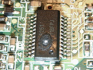
Electronic components have a wide range of failure modes. These can be classified in various ways, such as by time or cause. Failures can be caused by excess temperature, excess current or voltage, ionizing radiation, mechanical shock, stress or impact, and many other causes. In semiconductor devices, problems in the device package may cause failures due to contamination, mechanical stress of the device, or open or short circuits.

