Related Research Articles

Cathodoluminescence is an optical and electromagnetic phenomenon in which electrons impacting on a luminescent material such as a phosphor, cause the emission of photons which may have wavelengths in the visible spectrum. A familiar example is the generation of light by an electron beam scanning the phosphor-coated inner surface of the screen of a television that uses a cathode-ray tube. Cathodoluminescence is the inverse of the photoelectric effect, in which electron emission is induced by irradiation with photons.

Atomic force microscopy (AFM) or scanning force microscopy (SFM) is a very-high-resolution type of scanning probe microscopy (SPM), with demonstrated resolution on the order of fractions of a nanometer, more than 1000 times better than the optical diffraction limit.
Scanning probe microscopy (SPM) is a branch of microscopy that forms images of surfaces using a physical probe that scans the specimen. SPM was founded in 1981, with the invention of the scanning tunneling microscope, an instrument for imaging surfaces at the atomic level. The first successful scanning tunneling microscope experiment was done by Gerd Binnig and Heinrich Rohrer. The key to their success was using a feedback loop to regulate gap distance between the sample and the probe.

An X-ray microscope uses electromagnetic radiation in the X-ray band to produce magnified images of objects. Since X-rays penetrate most objects, there is no need to specially prepare them for X-ray microscopy observations.

A scanning transmission electron microscope (STEM) is a type of transmission electron microscope (TEM). Pronunciation is [stɛm] or [ɛsti:i:ɛm]. As with a conventional transmission electron microscope (CTEM), images are formed by electrons passing through a sufficiently thin specimen. However, unlike CTEM, in STEM the electron beam is focused to a fine spot which is then scanned over the sample in a raster illumination system constructed so that the sample is illuminated at each point with the beam parallel to the optical axis. The rastering of the beam across the sample makes STEM suitable for analytical techniques such as Z-contrast annular dark-field imaging, and spectroscopic mapping by energy dispersive X-ray (EDX) spectroscopy, or electron energy loss spectroscopy (EELS). These signals can be obtained simultaneously, allowing direct correlation of images and spectroscopic data.
A superlens, or super lens, is a lens which uses metamaterials to go beyond the diffraction limit. The diffraction limit is a feature of conventional lenses and microscopes that limits the fineness of their resolution depending on the illumination wavelength and the numerical aperture (NA) of the objective lens. Many lens designs have been proposed that go beyond the diffraction limit in some way, but constraints and obstacles face each of them.

Near-field scanning optical microscopy (NSOM) or scanning near-field optical microscopy (SNOM) is a microscopy technique for nanostructure investigation that breaks the far field resolution limit by exploiting the properties of evanescent waves. In SNOM, the excitation laser light is focused through an aperture with a diameter smaller than the excitation wavelength, resulting in an evanescent field on the far side of the aperture. When the sample is scanned at a small distance below the aperture, the optical resolution of transmitted or reflected light is limited only by the diameter of the aperture. In particular, lateral resolution of 6 nm and vertical resolution of 2–5 nm have been demonstrated.
Interference lithography is a technique that uses coherent light for patterning regular arrays of fine features without the use of complex optical systems or photomasks.

Feature-oriented scanning (FOS) is a method of precision measurement of surface topography with a scanning probe microscope in which surface features (objects) are used as reference points for microscope probe attachment. With FOS method, by passing from one surface feature to another located nearby, the relative distance between the features and the feature neighborhood topographies are measured. This approach allows to scan an intended area of a surface by parts and then reconstruct the whole image from the obtained fragments. Beside the mentioned, it is acceptable to use another name for the method – object-oriented scanning (OOS).
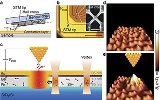
Scanning Hall probe microscope (SHPM) is a variety of a scanning probe microscope which incorporates accurate sample approach and positioning of the scanning tunnelling microscope with a semiconductor Hall sensor. Developed in 1996 by Oral, Bending and Henini, SHPM allows mapping the magnetic induction associated with a sample. Current state of the art SHPM systems utilize 2D electron gas materials to provide high spatial resolution (~300 nm) imaging with high magnetic field sensitivity. Unlike the magnetic force microscope the SHPM provides direct quantitative information on the magnetic state of a material. The SHPM can also image magnetic induction under applied fields up to ~1 tesla and over a wide range of temperatures.
Scanning confocal electron microscopy (SCEM) is an electron microscopy technique analogous to scanning confocal optical microscopy (SCOM). In this technique, the studied sample is illuminated by a focussed electron beam, as in other scanning microscopy techniques, such as scanning transmission electron microscopy or scanning electron microscopy. However, in SCEM, the collection optics are arranged symmetrically to the illumination optics to gather only the electrons that pass the beam focus. This results in superior depth resolution of the imaging. The technique is relatively new and is being actively developed.

Scanning thermal microscopy (SThM) is a type of scanning probe microscopy that maps the local temperature and thermal conductivity of an interface. The probe in a scanning thermal microscope is sensitive to local temperatures – providing a nano-scale thermometer. Thermal measurements at the nanometer scale are of both scientific and industrial interest. The technique was invented by Clayton C. Williams and H. Kumar Wickramasinghe in 1986.

Local oxidation nanolithography (LON) is a tip-based nanofabrication method. It is based on the spatial confinement on an oxidation reaction under the sharp tip of an atomic force microscope.
Surface-enhanced ellipsometric contrast microscopy (SEEC) uses an upright or inverted optical microscope in a crossed polarization configuration and specific supporting plates called surfs on which the sample is deposited for observation. It is described as an optical nanoscopy technique.
Super-resolution microscopy is a series of techniques in optical microscopy that allow such images to have resolutions higher than those imposed by the diffraction limit, which is due to the diffraction of light. Super-resolution imaging techniques rely on the near-field or on the far-field. Among techniques that rely on the latter are those that improve the resolution only modestly beyond the diffraction-limit, such as confocal microscopy with closed pinhole or aided by computational methods such as deconvolution or detector-based pixel reassignment, the 4Pi microscope, and structured-illumination microscopy technologies such as SIM and SMI.
Digital holographic microscopy (DHM) is digital holography applied to microscopy. Digital holographic microscopy distinguishes itself from other microscopy methods by not recording the projected image of the object. Instead, the light wave front information originating from the object is digitally recorded as a hologram, from which a computer calculates the object image by using a numerical reconstruction algorithm. The image forming lens in traditional microscopy is thus replaced by a computer algorithm. Other closely related microscopy methods to digital holographic microscopy are interferometric microscopy, optical coherence tomography and diffraction phase microscopy. Common to all methods is the use of a reference wave front to obtain amplitude (intensity) and phase information. The information is recorded on a digital image sensor or by a photodetector from which an image of the object is created (reconstructed) by a computer. In traditional microscopy, which do not use a reference wave front, only intensity information is recorded and essential information about the object is lost.

Photoconductive atomic force microscopy (PC-AFM) is a variant of atomic force microscopy that measures photoconductivity in addition to surface forces.
The technique of vibrational analysis with scanning probe microscopy allows probing vibrational properties of materials at the submicrometer scale, and even of individual molecules. This is accomplished by integrating scanning probe microscopy (SPM) and vibrational spectroscopy. This combination allows for much higher spatial resolution than can be achieved with conventional Raman/FTIR instrumentation. The technique is also nondestructive, requires non-extensive sample preparation, and provides more contrast such as intensity contrast, polarization contrast and wavelength contrast, as well as providing specific chemical information and topography images simultaneously.
Differential dynamic microscopy (DDM) is an optical technique that allows performing light scattering experiments by means of a simple optical microscope. DDM is suitable for typical soft materials such as for instance liquids or gels made of colloids, polymers and liquid crystals but also for biological materials like bacteria and cells.
A probe tip is an instrument used in scanning probe microscopes (SPMs) to scan the surface of a sample and make nano-scale images of surfaces and structures. The probe tip is mounted on the end of a cantilever and can be as sharp as a single atom. In microscopy, probe tip geometry and the composition of both the tip and the surface being probed directly affect resolution and imaging quality. Tip size and shape are extremely important in monitoring and detecting interactions between surfaces. SPMs can precisely measure electrostatic forces, magnetic forces, chemical bonding, Van der Waals forces, and capillary forces. SPMs can also reveal the morphology and topography of a surface.
References
- ↑ "Dr. Ravikiran Attota". Archived from the original on 2016-06-16. Retrieved 2017-07-13.
- ↑ "Research & Development World".
- ↑ Attota, Ravikiran. "Nanoscale Measurements With TSOM* Optical Method" (PDF). www.nist.gov.
- ↑ Ravikiran Attota; Ronald G. Dixson; Andras E. Vladár (2011-06-01). "Through-focus scanning optical microscopy". www.spiedigitallibrary.org. doi:10.1117/12.884706.
- ↑ Attota, R.; Bunday, B.; Vartanian, V. (2013). "Critical dimension metrology by through-focus scanning optical microscopy beyond the 22 nm node". Appl. Phys. Lett. 102 (22): 222107. Bibcode:2013ApPhL.102v2107A. doi: 10.1063/1.4809512 .
- ↑ Attota, R.; Dixson, R.G. (2014). "Resolving three-dimensional shape of sub-50 nm wide lines with nanometer-scale sensitivity using conventional optical microscopes". Appl. Phys. Lett. 105 (4): 043101. Bibcode:2014ApPhL.105d3101A. doi: 10.1063/1.4891676 .
- ↑ Attota, R.; Kavuri, P.P.; Kang, H.; Kasica, R.; Chen, L. (2014). "Nanoparticle size determination using optical microscopes". Appl. Phys. Lett. 105 (16): 163105. Bibcode:2014ApPhL.105p3105A. doi: 10.1063/1.4900484 .
- ↑ Kang, H.; Attota, R.; Tondare, V.; Vladar, A.E.; Kavuri, P. (2015). "A method to determine the number of nanoparticles in a cluster using conventional optical microscopes". Appl. Phys. Lett. 107 (10): 103106. Bibcode:2015ApPhL.107j3106K. doi:10.1063/1.4930994.
| | This optics-related article is a stub. You can help Wikipedia by expanding it. |