
In microelectronics, a dual in-line package, or dual in-line pin package (DIPP) is an electronic component package with a rectangular housing and two parallel rows of electrical connecting pins. The package may be through-hole mounted to a printed circuit board (PCB) or inserted in a socket. The dual-inline format was invented by Don Forbes, Rex Rice and Bryant Rogers at Fairchild R&D in 1964, when the restricted number of leads available on circular transistor-style packages became a limitation in the use of integrated circuits. Increasingly complex circuits required more signal and power supply leads ; eventually microprocessors and similar complex devices required more leads than could be put on a DIP package, leading to development of higher-density packages. Furthermore, square and rectangular packages made it easier to route printed-circuit traces beneath the packages.

Point-to-point construction is a non-automated method of construction of electronics circuits widely used before the use of printed circuit boards (PCBs) and automated assembly gradually became widespread following their introduction in the 1950s. Circuits using thermionic valves were relatively large, relatively simple, and used large sockets, all of which made the PCB less obviously advantageous than with later complex semiconductor circuits. Point-to-point construction is still used to construct prototype equipment with few or heavy electronic components.

Surface-mount technology (SMT) is a method for producing electronic circuits in which the components are mounted or placed directly onto the surface of printed circuit boards (PCBs). An electronic device so made is called a surface-mount device (SMD). In industry, it has largely replaced the through-hole technology construction method of fitting components with wire leads into holes in the circuit board. Both technologies can be used on the same board, with the through-hole technology used for components not suitable for surface mounting such as large transformers and heat-sinked power semiconductors.

Stripboard is the generic name for a widely used type of electronics prototyping board characterized by a 0.1 inches (2.54 mm) regular (rectangular) grid of holes, with wide parallel strips of copper cladding running in one direction all the way across one side of the board. It is commonly also known by the name of the original product Veroboard, which is a trademark, in the UK, of British company Vero Technologies Ltd and Canadian company Pixel Print Ltd. In using the board, breaks are made in the tracks, usually around holes, to divide the strips into multiple electrical nodes. With care, it is possible to break between holes to allow for components that have two pin rows only one position apart such as twin row headers for IDCs.
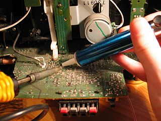
In electronics, desoldering is the removal of solder and components from a circuit board for troubleshooting, repair, replacement, and salvage.

Wave soldering is a bulk soldering process used in the manufacture of printed circuit boards. The circuit board is passed over a pan of molten solder in which a pump produces an upwelling of solder that looks like a standing wave. As the circuit board makes contact with this wave, the components become soldered to the board. Wave soldering is used for both through-hole printed circuit assemblies, and surface mount. In the latter case, the components are glued onto the surface of a printed circuit board (PCB) by placement equipment, before being run through the molten solder wave. Wave soldering is mainly used in soldering of through hole components.

Reflow soldering is a process in which a solder paste is used to temporarily attach one or thousands of tiny electrical components to their contact pads, after which the entire assembly is subjected to controlled heat. The solder paste reflows in a molten state, creating permanent solder joints. Heating may be accomplished by passing the assembly through a reflow oven or under an infrared lamp or by soldering individual joints [unconventionally] with a desoldering hot air pencil.
Rework is the term for the refinishing operation or repair of an electronic printed circuit board (PCB) assembly, usually involving desoldering and re-soldering of surface-mounted electronic components (SMD). Mass processing techniques are not applicable to single device repair or replacement, and specialized manual techniques by expert personnel using appropriate equipment are required to replace defective components; area array packages such as ball grid array (BGA) devices particularly require expertise and appropriate tools. A hot air gun or hot air station is used to heat devices and melt solder, and specialised tools are used to pick up and position often tiny components.
A via or VIA is an electrical connection between layers in a physical electronic circuit that goes through the plane of one or more adjacent layers. To ensure via robustness, IPC sponsored a round-robin exercise that developed a time to failure calculator.

Flat no-leads packages such as quad-flat no-leads (QFN) and dual-flat no-leads (DFN) physically and electrically connect integrated circuits to printed circuit boards. Flat no-leads, also known as micro leadframe (MLF) and SON, is a surface-mount technology, one of several package technologies that connect ICs to the surfaces of PCBs without through-holes. Flat no-lead is a near chip scale plastic encapsulated package made with a planar copper lead frame substrate. Perimeter lands on the package bottom provide electrical connections to the PCB. Flat no-lead packages include an exposed thermal pad to improve heat transfer out of the IC. Heat transfer can be further facilitated by metal vias in the thermal pad. The QFN package is similar to the quad-flat package (QFP), and a ball grid array (BGA).

Perfboard is a material for prototyping electronic circuits. It is a thin, rigid sheet with holes pre-drilled at standard intervals across a grid, usually a square grid of 0.1 inches (2.54 mm) spacing. These holes are ringed by round or square copper pads, though bare boards are also available. Inexpensive perfboard may have pads on only one side of the board, while better quality perfboard can have pads on both sides. Since each pad is electrically isolated, the builder makes all connections with either wire wrap or miniature point to point wiring techniques. Discrete components are soldered to the prototype board such as resistors, capacitors, and integrated circuits. The substrate is typically made of paper laminated with phenolic resin or a fiberglass-reinforced epoxy laminate (FR-4).

Bead probe technology (BPT) is technique used to provide electrical access to printed circuit board (PCB) circuitry for performing in-circuit testing (ICT). It makes use of small beads of solder placed onto the board's traces to allow measuring and controlling of the signals using a test probe. This permits test access to boards on which standard ICT test pads are not feasible due to space constraints.

The thermal copper pillar bump, also known as the "thermal bump", is a thermoelectric device made from thin-film thermoelectric material embedded in flip chip interconnects for use in electronics and optoelectronic packaging, including: flip chip packaging of CPU and GPU integrated circuits (chips), laser diodes, and semiconductor optical amplifiers (SOA). Unlike conventional solder bumps that provide an electrical path and a mechanical connection to the package, thermal bumps act as solid-state heat pumps and add thermal management functionality locally on the surface of a chip or to another electrical component. The diameter of a thermal bump is 238 μm and 60 μm high.
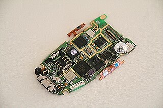
A semiconductor package is a metal, plastic, glass, or ceramic casing containing one or more discrete semiconductor devices or integrated circuits. Individual components are fabricated on semiconductor wafers before being diced into die, tested, and packaged. The package provides a means for connecting the package to the external environment, such as printed circuit board, via leads such as lands, balls, or pins; and protection against threats such as mechanical impact, chemical contamination, and light exposure. Additionally, it helps dissipate heat produced by the device, with or without the aid of a heat spreader. There are thousands of package types in use. Some are defined by international, national, or industry standards, while others are particular to an individual manufacturer.
Pad cratering is a mechanically induced fracture in the resin between copper foil and outermost layer of fiberglass of a printed circuit board (PCB). It may be within the resin or at the resin to fiberglass interface.

Chip on board is the method of manufacturing where integrated circuits are wired and bonded directly to a printed circuit board. By eliminating the packaging of individual semiconductor devices, the completed product can be more compact, lighter, and less costly. In some cases chip on board construction improves the operation of radio frequency systems by reducing the inductance and capacitance of integrated circuit leads. Chip on board effectively merges two levels of electronic packaging, level 1 (components) and level 2, and may be referred to as a "level 1.5"


