In electrical engineering, a ground plane is an electrically conductive surface, usually connected to electrical ground.

A printed circuit board (PCB), also called printed wiring board (PWB), is a laminated sandwich structure of conductive and insulating layers, each with a pattern of traces, planes and other features etched from one or more sheet layers of copper laminated onto or between sheet layers of a non-conductive substrate. PCBs are used to connect or "wire" components to one another in an electronic circuit. Electrical components may be fixed to conductive pads on the outer layers, generally by soldering, which both electrically connects and mechanically fastens the components to the board. Another manufacturing process adds vias, metal-lined drilled holes that enable electrical interconnections between conductive layers, to boards with more than a single side.

In electronics, point-to-point construction is a non-automated technique for constructing circuits which was widely used before the use of printed circuit boards (PCBs) and automated assembly gradually became widespread following their introduction in the 1950s. Circuits using thermionic valves were relatively large, relatively simple, and used large sockets, all of which made the PCB less obviously advantageous than with later complex semiconductor circuits. Point-to-point construction is still widespread in power electronics, where components are bulky and serviceability is a consideration, and to construct prototype equipment with few or heavy electronic components. A common practice, especially in older point-to-point construction, is to use the leads of components such as resistors and capacitors to bridge as much of the distance between connections as possible, reducing the need to add additional wire between the components.

Surface-mount technology (SMT), originally called planar mounting, is a method in which the electrical components are mounted directly onto the surface of a printed circuit board (PCB). An electrical component mounted in this manner is referred to as a surface-mount device (SMD). In industry, this approach has largely replaced the through-hole technology construction method of fitting components, in large part because SMT allows for increased manufacturing automation which reduces cost and improves quality. It also allows for more components to fit on a given area of substrate. Both technologies can be used on the same board, with the through-hole technology often used for components not suitable for surface mounting such as large transformers and heat-sinked power semiconductors.

Stripboard is the generic name for a widely used type of electronics prototyping material for circuit boards characterized by a pre-formed 0.1 inches (2.54 mm) regular (rectangular) grid of holes, with wide parallel strips of copper cladding running in one direction all the way along one side of an insulating bonded paper board. It is commonly also known by the name of the original product Veroboard, which is a trademark, in the UK, of British company Vero Technologies Ltd and Canadian company Pixel Print Ltd. It was originated and developed in the early 1960s by the Electronics Department of Vero Precision Engineering Ltd (VPE). It was introduced as a general-purpose material for use in constructing electronic circuits - differing from purpose-designed printed circuit boards (PCBs) in that a variety of electronics circuits may be constructed using a standard wiring board.
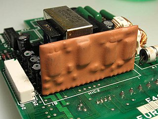
A hybrid integrated circuit (HIC), hybrid microcircuit, hybrid circuit or simply hybrid is a miniaturized electronic circuit constructed of individual devices, such as semiconductor devices and passive components, bonded to a substrate or printed circuit board (PCB). A PCB having components on a Printed wiring board (PWB) is not considered a true hybrid circuit according to the definition of MIL-PRF-38534.

A via is an electrical connection between two or more metal layers of a printed circuit boards (PCB) or integrated circuit. Essentially a via is a small drilled hole that goes through two or more adjacent layers; the hole is plated with metal that forms an electrical connection through the insulating layers.

Flat no-leads packages such as quad-flat no-leads (QFN) and dual-flat no-leads (DFN) physically and electrically connect integrated circuits to printed circuit boards. Flat no-leads, also known as micro leadframe (MLF) and SON, is a surface-mount technology, one of several package technologies that connect ICs to the surfaces of PCBs without through-holes. Flat no-lead is a near chip scale plastic encapsulated package made with a planar copper lead frame substrate. Perimeter lands on the package bottom provide electrical connections to the PCB. Flat no-lead packages usually, but not always, include an exposed thermally conductive pad to improve heat transfer out of the IC. Heat transfer can be further facilitated by metal vias in the thermal pad. The QFN package is similar to the quad-flat package (QFP), and a ball grid array (BGA).

Perfboard is a material for prototyping electronic circuits. It is a thin, rigid sheet with holes pre-drilled at standard intervals across a grid, usually a square grid of 0.1 inches (2.54 mm) spacing. These holes are ringed by round or square copper pads, though bare boards are also available. Inexpensive perfboard may have pads on only one side of the board, while better quality perfboard can have pads on both sides. Since each pad is electrically isolated, the builder makes all connections with either wire wrap or miniature point to point wiring techniques. Discrete components are soldered to the prototype board such as resistors, capacitors, and integrated circuits. The substrate is typically made of paper laminated with phenolic resin or a fiberglass-reinforced epoxy laminate (FR-4).

A thermal relief pad, thermal pad or simply thermal, is a printed circuit board (PCB) pad connected to a copper pour using a thermal connection. It looks like a normal pad with copper "spokes" connecting it to the surrounding copper.
Solder mask, solder stop mask or solder resist is a thin lacquer-like layer of polymer that is usually applied to the copper traces of a printed circuit board (PCB) for protection against oxidation and to prevent solder bridges from forming between closely spaced solder pads. Soldermask is a printed circuit board (PCB) manufacturing process that uses a chemical or thermosetting resin to coat a thin film on a circuit board, which can effectively form a layer of reliable protection to avoid unwanted short-circuiting and leakage of the circuit board, and to improve the reliability and electrical performance of the circuit board. A solder bridge is an unintended electrical connection between two conductors by means of a small blob of solder. PCBs use solder masks to prevent this from happening. Solder mask is not always used for hand soldered assemblies, but is essential for mass-produced boards that are soldered automatically using reflow or wave soldering techniques. Once applied, openings must be made in the solder mask wherever components are soldered, which is accomplished using photolithography. Solder mask is traditionally green, but is also available in many other colors.
Microvias are used as the interconnects between layers in high density interconnect (HDI) substrates and printed circuit boards (PCBs) to accommodate the high input/output (I/O) density of advanced packages.
The Occam process is a solder-free, Restriction of Hazardous Substances Directive (RoHS)-compliant method for use in circuit board manufacturing developed by Verdant Electronics. It combines the usual two steps of constructing printed circuit boards (PCBs) followed by the population process of placing various leaded and non-leaded electronic components into one process. The name "Occam" comes from a quotation by William of Ockham.
A via fence, also called a picket fence, is a structure used in planar electronic circuit technologies to improve isolation between components that would otherwise be coupled by electromagnetic fields. It consists of a row of via holes which, if spaced close enough together, form a barrier to electromagnetic wave propagation of slab modes in the substrate. Additionally if radiation in the air above the board is also to be suppressed, then a strip pad with via fence allows a shielding can to be electrically attached to the top side, but electrically behave as if it continued through the PCB.

DesignSpark PCB is a free electronic design automation software package for printed circuit boards. Although there is no charge for the software, the user must register with DesignSpark.com to unlock the program and it displays advertisements which must be acknowledged before the user can begin working.

DipTrace is a proprietary software suite for electronic design automation (EDA) used for electronic schematic capture and printed circuit board layouts. DipTrace has four applications: schematic editor, PCB editor with built-in shape-based autorouter and 3D preview, component editor, and pattern editor.
Stencil printing is the process of depositing solder paste on the printed wiring boards (PWBs) to establish electrical connections. It is immediately followed by the component placement stage. The equipment and materials used in this stage are a stencil, solder paste, and a printer.
In electronics, a cross section, cross-section, or microsection, is a prepared electronics sample that allows analysis at a plane that cuts through the sample. It is a destructive technique requiring that a portion of the sample be cut or ground away to expose the internal plane for analysis. They are commonly prepared for research, manufacturing quality assurance, supplier conformity, and failure analysis. Printed wiring boards (PWBs) and electronic components and their solder joints are common cross sectioned samples. The features of interest to be analyzed in cross section can be nanometer-scale metal and dielectric layers in semiconductors up to macroscopic features such as the amount of solder that has filled into a large, 0.125in (3.18mm) diameter plated-through hole.

In electronics, prototyping means building an actual circuit to a theoretical design to verify that it works, and to provide a physical platform for debugging it if it does not. The prototype is often constructed using techniques such as wire wrapping or using a breadboard, stripboard or perfboard, with the result being a circuit that is electrically identical to the design but not physically identical to the final product.

Printed circuit board manufacturing is the process of manufacturing bare printed circuit boards (PCBs) and then populating them with electronic components. It involves the full assembly of a board into a functional circuit board.

