
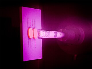
Chemical vapor deposition (CVD) is a vacuum deposition method used to produce high quality, and high-performance, solid materials. The process is often used in the semiconductor industry to produce thin films.

Microelectromechanical systems (MEMS), also written as micro-electro-mechanical systems and the related micromechatronics and microsystems constitute the technology of microscopic devices, particularly those with moving parts. They merge at the nanoscale into nanoelectromechanical systems (NEMS) and nanotechnology. MEMS are also referred to as micromachines in Japan and microsystem technology (MST) in Europe.
A viscometer is an instrument used to measure the viscosity of a fluid. For liquids with viscosities which vary with flow conditions, an instrument called a rheometer is used. Thus, a rheometer can be considered as a special type of viscometer. Viscometers only measure under one flow condition.
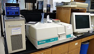
UV spectroscopy or UV–visible spectrophotometry refers to absorption spectroscopy or reflectance spectroscopy in part of the ultraviolet and the full, adjacent visible regions of the electromagnetic spectrum. Being relatively inexpensive and easily implemented, this methodology is widely used in diverse applied and fundamental applications. The only requirement is that the sample absorb in the UV-vis region, i.e. be a chromophore. Absorption spectroscopy is complementary to fluorescence spectroscopy. Parameters of interest, besides the wavelength of measurement, are absorbance (A) or Transmittance (%T) or Reflectance (%R), and its change with time.

A magnetometer is a device that measures magnetic field or magnetic dipole moment. Different types of magnetometers measure the direction, strength, or relative change of a magnetic field at a particular location. A compass is one such device, one that measures the direction of an ambient magnetic field, in this case, the Earth's magnetic field. Other magnetometers measure the magnetic dipole moment of a magnetic material such as a ferromagnet, for example by recording the effect of this magnetic dipole on the induced current in a coil.

A spectrum analyzer measures the magnitude of an input signal versus frequency within the full frequency range of the instrument. The primary use is to measure the power of the spectrum of known and unknown signals. The input signal that most common spectrum analyzers measure is electrical; however, spectral compositions of other signals, such as acoustic pressure waves and optical light waves, can be considered through the use of an appropriate transducer. Spectrum analyzers for other types of signals also exist, such as optical spectrum analyzers which use direct optical techniques such as a monochromator to make measurements.
A strain gauge is a device used to measure strain on an object. Invented by Edward E. Simmons and Arthur C. Ruge in 1938, the most common type of strain gauge consists of an insulating flexible backing which supports a metallic foil pattern. The gauge is attached to the object by a suitable adhesive, such as cyanoacrylate. As the object is deformed, the foil is deformed, causing its electrical resistance to change. This resistance change, usually measured using a Wheatstone bridge, is related to the strain by the quantity known as the gauge factor.
A thin film is a layer of material ranging from fractions of a nanometer (monolayer) to several micrometers in thickness. The controlled synthesis of materials as thin films is a fundamental step in many applications. A familiar example is the household mirror, which typically has a thin metal coating on the back of a sheet of glass to form a reflective interface. The process of silvering was once commonly used to produce mirrors, while more recently the metal layer is deposited using techniques such as sputtering. Advances in thin film deposition techniques during the 20th century have enabled a wide range of technological breakthroughs in areas such as magnetic recording media, electronic semiconductor devices, Integrated passive devices, LEDs, optical coatings, hard coatings on cutting tools, and for both energy generation and storage. It is also being applied to pharmaceuticals, via thin-film drug delivery. A stack of thin films is called a multilayer.

Ellipsometry is an optical technique for investigating the dielectric properties of thin films. Ellipsometry measures the change of polarization upon reflection or transmission and compares it to a model.
A quartz crystal microbalance (QCM) measures a mass variation per unit area by measuring the change in frequency of a quartz crystal resonator. The resonance is disturbed by the addition or removal of a small mass due to oxide growth/decay or film deposition at the surface of the acoustic resonator. The QCM can be used under vacuum, in gas phase and more recently in liquid environments. It is useful for monitoring the rate of deposition in thin film deposition systems under vacuum. In liquid, it is highly effective at determining the affinity of molecules to surfaces functionalized with recognition sites. Larger entities such as viruses or polymers are investigated as well. QCM has also been used to investigate interactions between biomolecules. Frequency measurements are easily made to high precision ; hence, it is easy to measure mass densities down to a level of below 1 μg/cm2. In addition to measuring the frequency, the dissipation factor is often measured to help analysis. The dissipation factor is the inverse quality factor of the resonance, Q−1 = w/fr ; it quantifies the damping in the system and is related to the sample's viscoelastic properties.
Atomic layer deposition (ALD) is a thin-film deposition technique based on the sequential use of a gas-phase chemical process; it is a subclass of chemical vapour deposition. The majority of ALD reactions use two chemicals called precursors. These precursors react with the surface of a material one at a time in a sequential, self-limiting, manner. A thin film is slowly deposited through repeated exposure to separate precursors. ALD is a key process in fabricating semiconductor devices, and part of the set of tools for synthesising nanomaterials.

Dip coating is an industrial coating process which is used, for example, to manufacture bulk products such as coated fabrics and condoms and specialised coatings for example in the biomedical field. Dip coating is also commonly used in academic research, where many chemical and nano material engineering research projects use the dip coating technique to create thin-film coatings.
Vacuum deposition is a group of processes used to deposit layers of material atom-by-atom or molecule-by-molecule on a solid surface. These processes operate at pressures well below atmospheric pressure. The deposited layers can range from a thickness of one atom up to millimeters, forming freestanding structures. Multiple layers of different materials can be used, for example to form optical coatings. The process can be qualified based on the vapor source; physical vapor deposition uses a liquid or solid source and chemical vapor deposition uses a chemical vapor.
Physical vapor deposition (PVD), sometimes called physical vapor transport (PVT), describes a variety of vacuum deposition methods which can be used to produce thin films and coatings. PVD is characterized by a process in which the material goes from a condensed phase to a vapor phase and then back to a thin film condensed phase. The most common PVD processes are sputtering and evaporation. PVD is used in the manufacture of items which require thin films for mechanical, optical, chemical or electronic functions. Examples include semiconductor devices such as thin film solar panels, aluminized PET film for food packaging and balloons, and titanium nitride coated cutting tools for metalworking. Besides PVD tools for fabrication, special smaller tools have been developed.

Evaporation is a common method of thin-film deposition. The source material is evaporated in a vacuum. The vacuum allows vapor particles to travel directly to the target object (substrate), where they condense back to a solid state. Evaporation is used in microfabrication, and to make macro-scale products such as metallized plastic film.
Within surface science, a quartz crystal microbalance with dissipation monitoring (QCM-D) is a type of quartz crystal microbalance (QCM) based on the ring-down technique. It is used in interfacial acoustic sensing. Its most common application is the determination of a film thickness in a liquid environment. It can be used to investigate further properties of the sample, most notably the layer's softness.
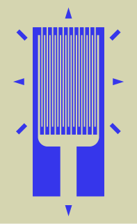
Surface acoustic wave sensors are a class of microelectromechanical systems (MEMS) which rely on the modulation of surface acoustic waves to sense a physical phenomenon. The sensor transduces an input electrical signal into a mechanical wave which, unlike an electrical signal, can be easily influenced by physical phenomena. The device then transduces this wave back into an electrical signal. Changes in amplitude, phase, frequency, or time-delay between the input and output electrical signals can be used to measure the presence of the desired phenomenon.
A. R. Forouhi and I. Bloomer deduced dispersion equations for the refractive index, n, and extinction coefficient, k, which were published in 1986 and 1988. The 1986 publication relates to amorphous materials, while the 1988 publication relates to crystalline. Subsequently, in 1991, their work was included as a chapter in “The Handbook of Optical Constants”. The Forouhi–Bloomer dispersion equations describe how photons of varying energies interact with thin films. When used with a spectroscopic reflectometry tool, the Forouhi–Bloomer dispersion equations specify n and k for amorphous and crystalline materials as a function of photon energy E. Values of n and k as a function of photon energy, E, are referred to as the spectra of n and k, which can also be expressed as functions of wavelength of light, λ, since E = hc/λ. The symbol h represents Planck’s constant and c, the speed of light in vacuum. Together, n and k are often referred to as the “optical constants” of a material.

Thermopile laser sensors are used for measuring laser power from a few µW to several W. The incoming radiation of the laser is converted into heat energy at the surface. This heat input produces a temperature gradient across the sensor. Making use of the thermoelectric effect a voltage is generated by this temperature gradient. Since the voltage is directly proportional to the incoming radiation, it can be directly related to the irradiation power.

Nanoparticle deposition refers to the process of attaching nanoparticles to solid surfaces called substrates to create coatings of nanoparticles. The coatings can have a monolayer or a multilayer and organized or unorganized structure based on the coating method used. Nanoparticles are typically difficult to deposit due to their physical properties.
