Related Research Articles

The 5ESS Switching System is a Class 5 telephone electronic switching system developed by Western Electric for the American Telephone and Telegraph Company (AT&T) and the Bell System in the United States. It came into service in 1982 and the last unit was produced in 2003.

Time-division multiplexing (TDM) is a method of transmitting and receiving independent signals over a common signal path by means of synchronized switches at each end of the transmission line so that each signal appears on the line only a fraction of time in an alternating pattern. It can be used when the bit rate of the transmission medium exceeds that of the signal to be transmitted. This form of signal multiplexing was developed in telecommunications for telegraphy systems in the late 19th century, but found its most common application in digital telephony in the second half of the 20th century.

In electronics and telecommunications, a crossbar switch is a collection of switches arranged in a matrix configuration. A crossbar switch has multiple input and output lines that form a crossed pattern of interconnecting lines between which a connection may be established by closing a switch located at each intersection, the elements of the matrix. Originally, a crossbar switch consisted literally of crossing metal bars that provided the input and output paths. Later implementations achieved the same switching topology in solid-state electronics. The crossbar switch is one of the principal telephone exchange architectures, together with a rotary switch, memory switch, and a crossover switch.

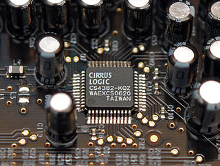
Dynamic random-access memory is a type of random-access semiconductor memory that stores each bit of data in a memory cell, usually consisting of a tiny capacitor and a transistor, both typically based on metal–oxide–semiconductor (MOS) technology. While most DRAM memory cell designs use a capacitor and transistor, some only use two transistors. In the designs where a capacitor is used, the capacitor can either be charged or discharged; these two states are taken to represent the two values of a bit, conventionally called 0 and 1. The electric charge on the capacitors gradually leaks away; without intervention the data on the capacitor would soon be lost. To prevent this, DRAM requires an external memory refresh circuit which periodically rewrites the data in the capacitors, restoring them to their original charge. This refresh process is the defining characteristic of dynamic random-access memory, in contrast to static random-access memory (SRAM) which does not require data to be refreshed. Unlike flash memory, DRAM is volatile memory, since it loses its data quickly when power is removed. However, DRAM does exhibit limited data remanence.
In electronics, a digital-to-analog converter is a system that converts a digital signal into an analog signal. An analog-to-digital converter (ADC) performs the reverse function.
A nonblocking minimal spanning switch is a device that can connect N inputs to N outputs in any combination. The most familiar use of switches of this type is in a telephone exchange. The term "non-blocking" means that if it is not defective, it can always make the connection. The term "minimal" means that it has the fewest possible components, and therefore the minimal expense.
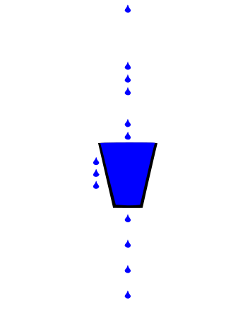
The leaky bucket is an algorithm based on an analogy of how a bucket with a constant leak will overflow if either the average rate at which water is poured in exceeds the rate at which the bucket leaks or if more water than the capacity of the bucket is poured in all at once. It can be used to determine whether some sequence of discrete events conforms to defined limits on their average and peak rates or frequencies, e.g. to limit the actions associated with these events to these rates or delay them until they do conform to the rates. It may also be used to check conformance or limit to an average rate alone, i.e. remove any variation from the average.
In electronics, a banyan switch is a complex crossover switch used in electrical or optical switches.

A network processor is an integrated circuit which has a feature set specifically targeted at the networking application domain.
In data communications, flow control is the process of managing the rate of data transmission between two nodes to prevent a fast sender from overwhelming a slow receiver. Flow control should be distinguished from congestion control, which is used for controlling the flow of data when congestion has actually occurred. Flow control mechanisms can be classified by whether or not the receiving node sends feedback to the sending node.

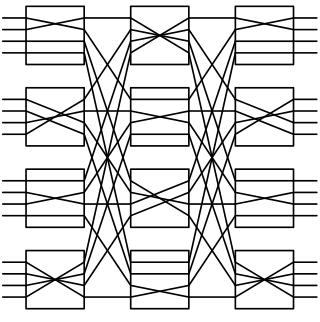
An Omega network is a network configuration often used in parallel computing architectures. It is an indirect topology that relies on the perfect shuffle interconnection algorithm.
In computer architecture, a transport triggered architecture (TTA) is a kind of processor design in which programs directly control the internal transport buses of a processor. Computation happens as a side effect of data transports: writing data into a triggering port of a functional unit triggers the functional unit to start a computation. This is similar to what happens in a systolic array. Due to its modular structure, TTA is an ideal processor template for application-specific instruction set processors (ASIP) with customized datapath but without the inflexibility and design cost of fixed function hardware accelerators.

An optical transport network (OTN) is a digital wrapper that encapsulates frames of data, to allow multiple data sources to be sent on the same channel. This creates an optical virtual private network for each client signal.
In the field of telecommunications, a Clos network is a kind of multistage circuit-switching network which represents a theoretical idealization of practical, multistage switching systems. It was invented by Edson Erwin in 1938 and first formalized by the American engineer Charles Clos in 1952.
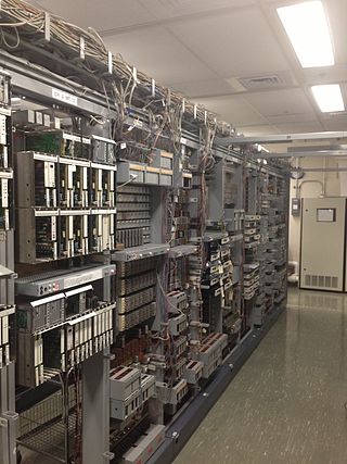
The Number One Electronic Switching System (1ESS) was the first large-scale stored program control (SPC) telephone exchange or electronic switching system in the Bell System. It was manufactured by Western Electric and first placed into service in Succasunna, New Jersey, in May 1965. The switching fabric was composed of a reed relay matrix controlled by wire spring relays which in turn were controlled by a central processing unit (CPU).
The No. 4 Electronic Switching System (4ESS) is a class 4 telephone electronic switching system that was the first digital electronic toll switch introduced by Western Electric for long-distance switching. It was introduced in Chicago in January 1976, to replace the 4A crossbar switch. The last of the 145 systems in the AT&T network was installed in 1999 in Atlanta. Approximately half of the switches were manufactured in Lisle, Illinois, and the other half in Oklahoma City, Oklahoma. At the time of the Bell System divestiture, most of the 4ESS switches became assets of AT&T as part of the long-distance network, while others remained in the RBOC networks. Over 140 4ESS switches remained in service in the United States in 2007.

Hiroshi Inose FREng was a Japanese electrical engineer, known as the inventor of the Time-Slot Interchange system (TSI), which is basic to modern digital telephone switches. Inose was highly involved within his career. He held positions such as director general, chairman, associate professor, and president specific committees pertaining to engineering and technology. He was awarded with many honorific titles. In 1976 he received the Marconi Prize, in 1993 the Harold Pender Award, and in 1994 the IEEE Alexander Graham Bell Medal.

In routing, the forwarding plane, sometimes called the data plane or user plane, defines the part of the router architecture that decides what to do with packets arriving on an inbound interface. Most commonly, it refers to a table in which the router looks up the destination address of the incoming packet and retrieves the information necessary to determine the path from the receiving element, through the internal forwarding fabric of the router, and to the proper outgoing interface(s).
Multistage interconnection networks (MINs) are a class of high-speed computer networks usually composed of processing elements (PEs) on one end of the network and memory elements (MEs) on the other end, connected by switching elements (SEs). The switching elements themselves are usually connected to each other in stages, hence the name.
This glossary of computer hardware terms is a list of definitions of terms and concepts related to computer hardware, i.e. the physical and structural components of computers, architectural issues, and peripheral devices.