
An integrated circuit or monolithic integrated circuit is a set of electronic circuits on one small flat piece of semiconductor material that is normally silicon. The integration of large numbers of tiny transistors into a small chip results in circuits that are orders of magnitude smaller, faster, and less expensive than those constructed of discrete electronic components. The IC's mass production capability, reliability, and building-block approach to circuit design has ensured the rapid adoption of standardized ICs in place of designs using discrete transistors. ICs are now used in virtually all electronic equipment and have revolutionized the world of electronics. Computers, mobile phones, and other digital home appliances are now inextricable parts of the structure of modern societies, made possible by the small size and low cost of ICs.

Semiconductor device fabrication is the process used to create the integrated circuits that are present in everyday electrical and electronic devices. It is a multiple-step sequence of photolithographic and chemical processing steps during which electronic circuits are gradually created on a wafer made of pure semiconducting material. Silicon is almost always used, but various compound semiconductors are used for specialized applications.
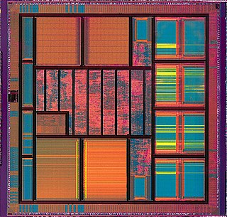
Very-large-scale integration (VLSI) is the process of creating an integrated circuit (IC) by combining millions of transistors or devices into a single chip. VLSI began in the 1970s when complex semiconductor and communication technologies were being developed. The microprocessor is a VLSI device. Before the introduction of VLSI technology most ICs had a limited set of functions they could perform. An electronic circuit might consist of a CPU, ROM, RAM and other glue logic. VLSI lets IC designers add all of these into one chip.

The Czochralski process is a method of crystal growth used to obtain single crystals of semiconductors, metals, salts and synthetic gemstones. The process is named after Polish scientist Jan Czochralski, who invented the method in 1915 while investigating the crystallization rates of metals. He made this discovery by accident, while studying the crystallization rate of metals: instead of dipping his pen into his inkwell, he dipped it in molten tin, and drew a tin filament, which later proved to be a single crystal.
Flip chip, also known as controlled collapse chip connection or its abbreviation, C4, is a method for interconnecting semiconductor devices, such as IC chips and microelectromechanical systems (MEMS), to external circuitry with solder bumps that have been deposited onto the chip pads. The technique was developed by General Electric's Light Military Electronics Dept., Utica, N.Y. The solder bumps are deposited on the chip pads on the top side of the wafer during the final wafer processing step. In order to mount the chip to external circuitry, it is flipped over so that its top side faces down, and aligned so that its pads align with matching pads on the external circuit, and then the solder is reflowed to complete the interconnect. This is in contrast to wire bonding, in which the chip is mounted upright and wires are used to interconnect the chip pads to external circuitry.
An epitaxial wafer is a wafer of semiconducting material made by epitaxial growth (epitaxy) for use in photonics, microelectronics, spintronics, or photovoltaics. The epi layer may be the same material as the substrate, typically monocrystaline silicon, or it may be a more exotic material with specific desirable qualities.
Wafer-scale integration, WSI for short, is a rarely used system of building very-large ined circuit networks that use an entire silicon wafer to produce a single "super-chip". Combining large size and reduced packaging, WSI was expected to lead to dramatically reduced costs for some systems, notably massively parallel supercomputers. The name is taken from the term very-large-scale integration, the current state of the art when WSI was being developed.

A solar cell, or photovoltaic cell, is an electrical device that converts the energy of light directly into electricity by the photovoltaic effect, which is a physical and chemical phenomenon. It is a form of photoelectric cell, defined as a device whose electrical characteristics, such as current, voltage, or resistance, vary when exposed to light. Individual solar cell devices can be combined to form modules, otherwise known as solar panels. In basic terms a single junction silicon solar cell can produce a maximum open-circuit voltage of approximately 0.5 to 0.6 volts.
A dicing saw is a kind of saw which employs a high-speed spindle fitted with an extremely thin diamond blade or diamond wire to dice, cut, or groove semiconductor wafers, silicon, glass, ceramic, crystal, and many other types of material.
In the context of manufacturing integrated circuits, wafer dicing is the process by which die are separated from a wafer of semiconductor following the processing of the wafer. The dicing process can involve scribing and breaking, mechanical sawing or laser cutting. All methods are typically automated to ensure precision and accuracy.
Following the dicing process the individual silicon chips are encapsulated into chip carriers which are then suitable for use in building electronic devices such as computers, etc.

A diamond tool is a cutting tool with diamond grains fixed on the functional parts of the tool via a bonding material or another method. As diamond is a superhard material, diamond tools have many advantages as compared with tools made with common abrasives such as corundum and silicon carbide.

A die, in the context of integrated circuits, is a small block of semiconducting material on which a given functional circuit is fabricated. Typically, integrated circuits are produced in large batches on a single wafer of electronic-grade silicon (EGS) or other semiconductor through processes such as photolithography. The wafer is cut (diced) into many pieces, each containing one copy of the circuit. Each of these pieces is called a die.

Etching is used in microfabrication to chemically remove layers from the surface of a wafer during manufacturing. Etching is a critically important process module, and every wafer undergoes many etching steps before it is complete.
In microelectronics, a three-dimensional integrated circuit is an integrated circuit manufactured by stacking silicon wafers or dies and interconnecting them vertically using, for instance, through-silicon vias (TSVs) or Cu-Cu connections, so that they behave as a single device to achieve performance improvements at reduced power and smaller footprint than conventional two dimensional processes. 3D IC is just one of a host of 3D integration schemes that exploit the z-direction to achieve electrical performance benefits.
Ribbon solar cells are a 1970s technology most recently sold by Evergreen Solar, among other manufacturers.
Monocrystalline silicon is the base material for silicon-based discrete components and integrated circuits used in virtually all modern electronic equipment. Mono-Si also serves as a photovoltaic, light-absorbing material in the manufacture of solar cells.

Embedded Wafer Level Ball Grid Array (eWLB) is a packaging technology for integrated circuits. The package interconnects are applied on an artificial wafer made of silicon chips and a casting compound.
