Artificial lattice

Last updated

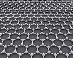
Artificial lattice is a term encompassing every atomic-scale structures designed and controlled to confine electrons onto a chosen lattice. Research has been done on multiple geometries and one of the most notable being what is called molecular graphene (in order to mimic graphene structure). Molecular graphene is a part of two-dimensional artificial lattices.

Contents

Artificial lattices can be studied to test theoretical topology predictions or for their engineered electronic proprieties. Those materials should still be considered at a research stage.

Synthesis

Synthesis of such materials is often achieved using Atomic manipulation by scanning tunneling microscope or atomic force microscope. [1] More and more efforts are being made to achieve a similar atomic precision with focused electron beams. [2] Those methods aren't adapted for a mass production of nanostructures as each molecule has to be moved one by one. To solve this issue, new methods of synthesize those compounds are being researched such as chemical bottom-up synthesis.

Currently, multiple methods, often complementary, exist for synthesizing such materials :

In the case of molecular graphene, carbon monoxide molecules on Cu(111) surface can be used. Other materials have been shown to be suitable for making molecular graphene suchlike Coronene. [3] Substrates such as Cu(111) are interesting because they have a 2D free-electron-like surface state. If CO molecules are placed onto appropriate positions, as the Cu(111) surface state is scattered from the CO molecules, the surface state electron gas can be confined onto different geometries (e.g. a honeycomb).

Proprieties

The main interest of artificial lattice is that its lattice proprieties (such as the lattice spacing) can be precisely controlled. In the case of molecular graphene, similarities in structure with graphene can provide an indirect to study graphene proprieties. Using a triaxial strain , it is possible to study how graphene react to intense magnetic fields. This strain (creating what is called a pseudo magnetic field) will alter the electronic structure of the molecule in the same fashion a magnetic field would. With this method, we can study how graphene would react to field up to 60 T. [4]

Some artificial lattices, such as molecular graphene, also exhibits semi-conductors' behaviors. PNP junctions can be made with the juxtaposition of two artificial graphene lattices with different lattice spacing. Indeed, Fermi level of a molecular graphene is directly linked to its lattice spacing. [1]

Graphene is a lattice that can be mimicked in artificial lattices Graphen.jpg
Graphene is a lattice that can be mimicked in artificial lattices

Multiple geometries for artificial lattices has been researched and created. Some of those geometries are :

Some of those geometries have a non-integer Hausdorff dimension as they are fractals. Those dimensions can be approximated using box counting methods. This dimension will dictate how electrons of the artificial lattice will behave and move in space. [1]

See also

Notes

1. ^ Bottom-up synthesis are chemical processes used in nanotechnologies to create nanoparticles. The principle is to start from atoms, then to gather them in clusters of atoms which will be finally merged into nanoparticles.
2. ^ Triaxial strain is obtained in molecular graphene with a modification of the arrangement of molecules.

Related Research Articles

Crystallographic defect Disruption of the periodicity of a crystal lattice

Crystallographic defects are interruptions of regular patterns in crystalline solids. They are common because positions of atoms or molecules at repeating fixed distances determined by the unit cell parameters in crystals, which exhibit a periodic crystal structure, are usually imperfect.

Molecule Electrically neutral group of two or more atoms

A molecule is a group of two or more atoms held together by attractive forces known as chemical bonds; depending on context, the term may or may not include ions which satisfy this criterion. In quantum physics, organic chemistry, and biochemistry, the distinction from ions is dropped and molecule is often used when referring to polyatomic ions.

Molecular electronics is the study and application of molecular building blocks for the fabrication of electronic components. It is an interdisciplinary area that spans physics, chemistry, and materials science. The unifying feature is use of molecular building blocks to fabricate electronic components. Due to the prospect of size reduction in electronics offered by molecular-level control of properties, molecular electronics has generated much excitement. It provides a potential means to extend Moore's Law beyond the foreseen limits of small-scale conventional silicon integrated circuits.

Electron diffraction

Electron diffraction is a phenomenon of electron beam bending around atomic structures. This behaviour typical for waves is applicable to electrons due to the wave–particle duality stating that electrons behave as both, particles and waves. Since the diffracted beams interfere, they generate diffraction patterns widely used for analysis of the objects which caused the diffraction. Therefore, electron diffraction can also refer to derived experimental techniques used for material characterization. This technique is similar to X-ray and neutron diffraction.

Reflection high-energy electron diffraction (RHEED) is a technique used to characterize the surface of crystalline materials. RHEED systems gather information only from the surface layer of the sample, which distinguishes RHEED from other materials characterization methods that also rely on diffraction of high-energy electrons. Transmission electron microscopy, another common electron diffraction method samples the bulk of the sample due to the geometry of the system. Low-energy electron diffraction (LEED) is also surface sensitive, but LEED achieves surface sensitivity through the use of low energy electrons.

Graphene Hexagonal lattice made of carbon atoms

Graphene is an allotrope of carbon consisting of a single layer of atoms arranged in a two-dimensional honeycomb lattice nanostructure. The name is derived from "graphite" and the suffix -ene, reflecting the fact that the graphite allotrope of carbon contains numerous double bonds.

A superlattice is a periodic structure of layers of two materials. Typically, the thickness of one layer is several nanometers. It can also refer to a lower-dimensional structure such as an array of quantum dots or quantum wires.

Transmission Electron Aberration-Corrected Microscope

Transmission Electron Aberration-Corrected Microscope (TEAM) is a collaborative research project between four US laboratories and two companies. The project's main activity is design and application of a transmission electron microscope (TEM) with a spatial resolution below 0.05 nanometers, which is roughly half the size of an atom of hydrogen.

Scanning transmission electron microscopy

A scanning transmission electron microscope (STEM) is a type of transmission electron microscope (TEM). Pronunciation is [stɛm] or [ɛsti:i:ɛm]. As with a conventional transmission electron microscope (CTEM), images are formed by electrons passing through a sufficiently thin specimen. However, unlike CTEM, in STEM the electron beam is focused to a fine spot which is then scanned over the sample in a raster illumination system constructed so that the sample is illuminated at each point with the beam parallel to the optical axis. The rastering of the beam across the sample makes STEM suitable for analytical techniques such as Z-contrast annular dark-field imaging, and spectroscopic mapping by energy dispersive X-ray (EDX) spectroscopy, or electron energy loss spectroscopy (EELS). These signals can be obtained simultaneously, allowing direct correlation of images and spectroscopic data.

Optical lattice

An optical lattice is formed by the interference of counter-propagating laser beams, creating a spatially periodic polarization pattern. The resulting periodic potential may trap neutral atoms via the Stark shift. Atoms are cooled and congregate at the potential extrema. The resulting arrangement of trapped atoms resembles a crystal lattice and can be used for quantum simulation.

Nanochemistry is the combination of chemistry and nano science. Nanochemistry is associated with synthesis of building blocks which are dependent on size, surface, shape and defect properties. Nanochemistry is being used in chemical, materials and physical, science as well as engineering, biological and medical applications. Nanochemistry and other nanoscience fields have the same core concepts but the usages of those concepts are different.

A two-dimensional gas is a collection of objects constrained to move in a planar or other two-dimensional space in a gaseous state. The objects can be: classical ideal gas elements such as rigid disks undergoing elastic collisions; elementary particles, or any ensemble of individual objects in physics which obeys laws of motion without binding interactions. The concept of a two-dimensional gas is used either because:

  1. the issue being studied actually takes place in two dimensions ; or,
  2. the two-dimensional form of the problem is more tractable than the analogous mathematically more complex three-dimensional problem.
Graphene nanoribbon Carbon allotrope

Graphene nanoribbons are strips of graphene with width less than 100 nm. Graphene ribbons were introduced as a theoretical model by Mitsutaka Fujita and coauthors to examine the edge and nanoscale size effect in graphene.

A crystallographic database is a database specifically designed to store information about the structure of molecules and crystals. Crystals are solids having, in all three dimensions of space, a regularly repeating arrangement of atoms, ions, or molecules. They are characterized by symmetry, morphology, and directionally dependent physical properties. A crystal structure describes the arrangement of atoms, ions, or molecules in a crystal.

Nanoarchitectonics

Nanoarchitectonics is a technology allowing to arrange nano-sized structural units, usually a group of atoms or molecules, in an intended configuration. It employs two major processes: nano-creation and nano-organization. Nano-organization involves re-arrangement of the structural units in a desired pattern, while nano-creation is synthesis of new materials that do not exist in nature. For example, by peeling atomic sheets off graphite slab, a novel nano-material graphene can be obtained, which has very different properties from graphite.

Length measurement, distance measurement, or range measurement (ranging) refers to the many ways in which length, distance, or range can be measured. The most commonly used approaches are the rulers, followed by transit-time methods and the interferometer methods based upon the speed of light.

In materials science, the term single-layer materials or 2D materials refers to crystalline solids consisting of a single layer of atoms. These materials are promising for some applications but remain the focus of research. Single-layer materials derived from single elements generally carry the -ene suffix in their names, e.g. graphene. Single-layer materials that are compounds of two or more elements have -ane or -ide suffixes. 2D materials can generally be categorized as either 2D allotropes of various elements or as compounds.

Band-gap engineering is the process of controlling or altering the band gap of a material. This is typically done to semiconductors by controlling the composition of alloys or constructing layered materials with alternating compositions. A band gap is the range in a solid where no electron state can exist. The band gap of insulators is much larger than in semiconductors. Conductors or metals have a much smaller or nonexistent band gap than semiconductors since the valence and conduction bands overlap. Controlling the band gap allows for the creation of desirable electrical properties.

This glossary of nanotechnology is a list of definitions of terms and concepts relevant to nanotechnology, its sub-disciplines, and related fields.

Atomic manipulation is the process of moving single atoms on a substrate using Scanning Tunneling Microscope (STM). The atomic manipulation is a surface science technique usually used to create artificial objects on the substrate made out of atoms and to study electronic behaviour of matter. These objects do not occur in nature and therefore need to be created artificially. The first demonstration of atomic manipulation was done by IBM scientists in 1989, when they created IBM in atoms.

References

  1. 1 2 3 4 5 6 7 8 Yan, Linghao; Liljeroth, Peter (2019). "Engineered electronic states in atomically precise artificial lattices and graphene nanoribbons". Advances in Physics: X. 4 (1): 29. arXiv: 1905.03328 . Bibcode:2019AdPhX...451672Y. doi:10.1080/23746149.2019.1651672. S2CID   198968312.
  2. Dyck, Ondrej; Maxim, Ziatdinov; et al. (2019). "Atom-by-atom fabrication with electron beams". Nature Reviews Materials. 4 (7): 497–507. Bibcode:2019NatRM...4..497D. doi:10.1038/s41578-019-0118-z. OSTI   1607230. S2CID   189930403.
  3. Wang, Shiyong; Tan, Liang Z.; et al. (2014). "Manipulation and Characterization of Aperiodical Graphene Structures Created in a Two-Dimensional Electron Gas". Physical Review Letters. 113 (19): 196803. Bibcode:2014PhRvL.113s6803W. doi: 10.1103/PhysRevLett.113.196803 . PMID   25415917.
  4. 1 2 Khajetoorians, Alexander A.; Wegner, Daniel; et al. (2019). "Creating designer quantum states of matter atom-by-atom". Nature Reviews Physics. 1 (12): 703–715. arXiv: 1904.11680 . Bibcode:2019NatRP...1..703K. doi:10.1038/s42254-019-0108-5. S2CID   135467867.