Related Research Articles

Solder is a fusible metal alloy used to create a permanent bond between metal workpieces. Solder is melted in order to wet the parts of the joint, where it adheres to and connects the pieces after cooling. Metals or alloys suitable for use as solder should have a lower melting point than the pieces to be joined. The solder should also be resistant to oxidative and corrosive effects that would degrade the joint over time. Solder used in making electrical connections also needs to have favorable electrical characteristics.

Electroplating, also known as electrochemical deposition or electrodeposition, is a process for producing a metal coating on a solid substrate through the reduction of cations of that metal by means of a direct electric current. The part to be coated acts as the cathode of an electrolytic cell; the electrolyte is a solution of a salt of the metal to be coated; and the anode is usually either a block of that metal, or of some inert conductive material. The current is provided by an external power supply.

A printed circuit board (PCB), also called printed wiring board (PWB), is a medium used to connect or "wire" components to one another in a circuit. It takes the form of a laminated sandwich structure of conductive and insulating layers: each of the conductive layers is designed with an artwork pattern of traces, planes and other features etched from one or more sheet layers of copper laminated onto and/or between sheet layers of a non-conductive substrate. Electrical components may be fixed to conductive pads on the outer layers in the shape designed to accept the component's terminals, generally by means of soldering, to both electrically connect and mechanically fasten them to it. Another manufacturing process adds vias, plated-through holes that allow interconnections between layers.

A ball grid array (BGA) is a type of surface-mount packaging used for integrated circuits. BGA packages are used to permanently mount devices such as microprocessors. A BGA can provide more interconnection pins than can be put on a dual in-line or flat package. The whole bottom surface of the device can be used, instead of just the perimeter. The traces connecting the package's leads to the wires or balls which connect the die to package are also on average shorter than with a perimeter-only type, leading to better performance at high speeds.
Plating is a finishing process in which a metal is deposited on a surface. Plating has been done for hundreds of years; it is also critical for modern technology. Plating is used to decorate objects, for corrosion inhibition, to improve solderability, to harden, to improve wearability, to reduce friction, to improve paint adhesion, to alter conductivity, to improve IR reflectivity, for radiation shielding, and for other purposes. Jewelry typically uses plating to give a silver or gold finish.

Gold plating is a method of depositing a thin layer of gold onto the surface of another metal, most often copper or silver, by chemical or electrochemical plating. This article covers plating methods used in the modern electronics industry; for more traditional methods, often used for much larger objects, see gilding.
A via is an electrical connection between two or more metal layers, and are commonly used in printed circuit boards (PCB). Essentially a via is a small drilled hole that goes through two or more adjacent layers; the hole is plated with metal that forms an electrical connection through the insulating layers.

Electroless deposition (ED) or electroless plating is defined as the autocatalytic process through which metals and metal alloys are deposited onto conductive and nonconductive surfaces. These nonconductive surfaces include plastics, ceramics, and glass etc., which can then become decorative, anti-corrosive, and conductive depending on their final functions. Electroplating unlike electroless deposition only deposits on other conductive or semi-conductive materials when a external current is applied. Electroless deposition deposits metals onto 2D and 3D structures such as screws, nanofibers, and carbon nanotubes, unlike other plating methods such as Physical Vapor Deposition ( PVD), Chemical Vapor Deposition (CVD), and electroplating, which are limited to 2D surfaces. Commonly the surface of the substrate is characterized via pXRD, SEM-EDS, and XPS which relay set parameters based their final funtionality. These parameters are referred to a Key Performance Indicators crucial for a researcher’ or company's purpose. Electroless deposition continues to rise in importance within the microelectronic industry, oil and gas, and aerospace industry.

Electroless nickel-phosphorus plating, also referred to as E-nickel, is a chemical process that deposits an even layer of nickel-phosphorus alloy on the surface of a solid substrate, like metal or plastic. The process involves dipping the substrate in a water solution containing nickel salt and a phosphorus-containing reducing agent, usually a hypophosphite salt. It is the most common version of electroless nickel plating and is often referred by that name. A similar process uses a borohydride reducing agent, yielding a nickel-boron coating instead.
HASL or HAL is a type of finish used on printed circuit boards (PCBs).
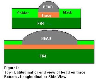
Bead probe technology (BPT) is technique used to provide electrical access to printed circuit board (PCB) circuitry for performing in-circuit testing (ICT). It makes use of small beads of solder placed onto the board's traces to allow measuring and controlling of the signals using a test probe. This permits test access to boards on which standard ICT test pads are not feasible due to space constraints.
Immersion silver plating is a surface plating process that creates a thin layer of silver over copper objects. It consists in dipping the object briefly into a solution containing silver ions.
Organic solderability preservative or OSP is a method for coating of printed circuit boards. It uses a water-based organic compound that selectively bonds to copper and protects the copper until soldering.
Nickel electroplating is a technique of electroplating a thin layer of nickel onto a metal object. The nickel layer can be decorative, provide corrosion resistance, wear resistance, or used to build up worn or undersized parts for salvage purposes.
Pad cratering is a mechanically induced fracture in the resin between copper foil and outermost layer of fiberglass of a printed circuit board (PCB). It may be within the resin or at the resin to fiberglass interface.

Electroless nickel-boron coating is a metal plating process that can create a layer of a nickel-boron alloy on the surface of a solid substrate, like metal or plastic. The process involves dipping the substrate in a water solution containing nickel salt and a boron-containing reducing agent, such as an alkylamineborane or sodium borohydride. It is a type of electroless nickel plating. A similar process, that uses a hypophosphite as a reducing agent, yields a nickel-phosphorus coating instead.
Stencil printing is the process of depositing solder paste on the printed wiring boards (PWBs) to establish electrical connections. It is immediately followed by the component placement stage. The equipment and materials used in this stage are a stencil, solder paste, and a printer.
Dye-n-Pry, also called Dye And Pry, Dye and Pull, Dye Staining, or Dye Penetrant, is a destructive analysis technique used on surface mount technology (SMT) components to either perform failure analysis or inspect for solder joint integrity. It is an application of dye penetrant inspection.
Electroless copper plating is a chemical process that deposits an even layer of copper on the surface of a solid substrate, like metal or plastic. The process involves dipping the substrate in a water solution containing copper salts and a reducing agent such as formaldehyde.
Immersion zinc plating is an electroless (non-electrolytic) coating process that deposits a thin layer of zinc on a less electronegative metal, by immersion in a solution containing a zinc or zincate ions, Zn(OH)2−
4. A typical use is plating aluminum with zinc prior to electrolytic or electroless nickel plating.
References
- 1 2 "Surface Finishes in a Lead Free World". Uyemura International Corporation. Retrieved 6 March 2019.
- ↑ IPC Plating Processes Subcommittee (2017): "Performance Specification for Electroless Nickel/Immersion Gold (ENIG) Plating for Printed Boards". Standard IPC-4552A; first version issued in 2002, amended in 2012.
- ↑ IPC Plating Processes Subcommittee (2017): "Design and Assembly Process Implementation for Ball Grid Arrays (BGAs)". Standard IPC-7095D; first version issued in 2000, amended in 2004, 2008, and 2013.
| | This metalworking article is a stub. You can help Wikipedia by expanding it. |