Electronic packaging

Last updated

Electronic packaging is the design and production of enclosures for electronic devices ranging from individual semiconductor devices up to complete systems such as a mainframe computer. Packaging of an electronic system must consider protection from mechanical damage, cooling, radio frequency noise emission and electrostatic discharge. Product safety standards may dictate particular features of a consumer product, for example, external case temperature or grounding of exposed metal parts. Prototypes and industrial equipment made in small quantities may use standardized commercially available enclosures such as card cages or prefabricated boxes. Mass-market consumer devices may have highly specialized packaging to increase consumer appeal. Electronic packaging is a major discipline within the field of mechanical engineering.

Contents

Design

Electronic packaging can be organized by levels:

The same electronic system may be packaged as a portable device or adapted for fixed mounting in an instrument rack or permanent installation. Packaging for aerospace, marine, or military systems imposes different types of design criteria.

Design and productisation of electronic packages is a multi-disciplinary field based on mechanical engineering principles such as dynamics, stress analysis, heat transfer and fluid mechanics, chemistry, materials science, process engineering, etc. High-reliability equipment often must survive drop tests, loose cargo vibration, secured cargo vibration, extreme temperatures, humidity, water immersion or spray, rain, sunlight (UV, IR and visible light), salt spray, explosive shock, and many more. These requirements extend beyond and interact with the electrical design.

An electronics assembly consists of component devices, circuit card assemblies (CCAs), connectors, cables and components such as transformers, power supplies, relays, switches, etc. that may not mount on the circuit card.

Many electrical products require the manufacturing of high-volume, low-cost parts such as enclosures or covers by techniques such as injection molding, die casting, investment casting, and so on. The design of these products depends on the production method and require careful consideration of dimensions and tolerances and tooling design. Some parts may be manufactured by specialized processes such as plaster- and sand-casting of metal enclosures.

In the design of electronic products, electronic packaging engineers perform analyses to estimate such things as maximum temperatures for components, structural resonant frequencies, and dynamic stresses and deflections under worst-case environments. Such knowledge is important to prevent immediate or premature electronic product failures.

Design considerations

A designer must balance many objectives and practical considerations when selecting packaging methods.

Packaging materials

Sheet metal

Punched and formed sheet metal is one of the oldest types of electronic packaging. It can be mechanically strong, provides electromagnetic shielding when the product requires that feature, and is easily made for prototypes and small production runs with little custom tooling expense.

Cast metal

Gasketed metal castings are sometimes used to package electronic equipment for exceptionally severe environments, such as in heavy industry, aboard ship, or deep under water. Aluminum die castings are more common than iron or steel sand castings.

Machined metal

Electronic packages are sometimes made by machining solid blocks of metal, usually aluminum, into complex shapes. They are fairly common in microwave assemblies for aerospace use, where precision transmission lines require complex metal shapes, in combination with hermetically sealed housings. Quantities tend to be small; sometimes only one unit of a custom design is required. Piece part costs are high, but there is little or no cost for custom tooling, and first-piece deliveries can take as little as half a day. The tool of choice is a numerically controlled vertical milling machine, with automatic translation of computer-aided design (CAD) files to toolpath command files.

Molded plastic

Molded plastic cases and structural parts can be made by a variety of methods, offering tradeoffs in piece part cost, tooling cost, mechanical and electrical properties, and ease of assembly. Examples are injection molding, transfer molding, vacuum forming, and die cutting. Pl can be post-processed to provide conductive surfaces.

Potting

Also called "encapsulation", potting consists of immersing the part or assembly in a liquid resin, then curing it. Another method puts the part or assembly in a mold, and potting compound is poured in it, and after curing, the mold is not removed, becoming part of the part or assembly. Potting can be done in a pre-molded potting shell, or directly in a mold. Today it is most widely used to protect semiconductor components from moisture and mechanical damage, and to serve as a mechanical structure holding the lead frame and the chip together. In earlier times it was often used to discourage reverse engineering of proprietary products built as printed circuit modules. It is also commonly used in high voltage products to allow live parts to be placed closer together (eliminating corona discharges due to the potting compound's high dielectric strength), so that the product can be smaller. This also excludes dirt and conductive contaminants (such as impure water) from sensitive areas. Another use is to protect deep-submergence items such as sonar transducers from collapsing under extreme pressure, by filling all voids. Potting can be rigid or soft. When void-free potting is required, it is common practice to place the product in a vacuum chamber while the resin is still liquid, hold a vacuum for several minutes to draw the air out of internal cavities and the resin itself, then release the vacuum. Atmospheric pressure collapses the voids and forces the liquid resin into all internal spaces. Vacuum potting works best with resins that cure by polymerization, rather than solvent evaporation.

Porosity sealing or impregnation

Porosity Sealing or Resin Impregnation is similar to potting, but doesn't use a shell or a mold. Parts are submerged in a polymerizable monomer or solvent-based low viscosity plastic solution. The pressure above the fluid is lowered to a full vacuum. After the vacuum is released, the fluid flows into the part. When the part is withdrawn from the resin bath, it is drained and/or cleaned and then cured. Curing can consist of polymerizing the internal resin or evaporating the solvent, which leaves an insulating dielectric material between different voltage components. Porosity sealing (Resin Impregnation) fills all interior spaces, and may or may not leave a thin coating on the surface, depending on the wash/rinse performance. The main application of vacuum impregnation porosity sealing is in boosting the dielectric strength of transformers, solenoids, lamination stacks or coils, and some high voltage components. It prevents ionization from forming between closely spaced live surfaces and initiating failure.

Liquid filling

Liquid filling is sometimes used as an alternative to potting or impregnation. It's usually a dielectric fluid, chosen for chemical compatibility with the other materials present. This method is used mostly in very large electrical equipment such as utility transformers, to increase breakdown voltage. It can also be used to improve heat transfer, especially if allowed to circulate by natural convection or forced convection through a heat exchanger. Liquid filling can be removed for repair much more easily than potting.

Conformal coating

Conformal coating is a thin insulating coating applied by various methods. It provides mechanical and chemical protection of delicate components. It's widely used on mass-produced items such as axial-lead resistors, and sometimes on printed circuit boards. It can be very economical, but somewhat difficult to achieve consistent process quality.

Glob-top

A chip-on-board (COB) covered with dark epoxy Famicom clone PCB.jpg
A chip-on-board (COB) covered with dark epoxy

Glob-top is a variant of conformal coating used in chip-on-board assembly (COB). It consists of a drop of specially formulated epoxy [3] or resin deposited over a semiconductor chip and its wire bonds, to provide mechanical support and exclude contaminants such as fingerprint residues which could disrupt circuit operation. It is most commonly used in electronic toys and low-end devices. [4]

Chip on board

Surface-mounted LEDs are frequently sold in chip-on-board (COB) configurations. In these, the individual diodes are mounted in an array that allows the device to produce a greater amount of luminous flux with greater ability to dissipate the resulting heat in an overall smaller package than can be accomplished by mounting LEDs, even surface mount types, individually on a circuit board. [5]

Hermetic metal/glass cases

Hermetic metal packaging began life in the vacuum tube industry, where a totally leak-proof housing was essential to operation. This industry developed the glass-seal electrical feedthrough, using alloys such as Kovar to match the coefficient of expansion of the sealing glass so as to minimize mechanical stress on the critical metal-glass bond as the tube warmed up. Some later tubes used metal cases and feedthroughs, and only the insulation around the individual feedthroughs used glass. Today, glass-seal packages are used mostly in critical components and assemblies for aerospace use, where leakage must be prevented even under extreme changes in temperature, pressure, and humidity.

Hermetic ceramic packages

Packages consisting of a lead frame embedded in a vitreous paste layer between flat ceramic top and bottom covers are more convenient than metal/glass packages for some products, but give equivalent performance. Examples are integrated circuit chips in ceramic Dual In-line Package form, or complex hybrid assemblies of chip components on a ceramic base plate. This type of packaging can also be divided into two main types: multilayer ceramic packages (like LTCC and HTCC) and pressed ceramic packages.

Printed circuit assemblies

Printed circuits are primarily a technology for connecting components together, but they also provide mechanical structure. In some products, such as computer accessory boards, they're all the structure there is. This makes them part of the universe of electronic packaging.

Electronic Packaging Small Form Factor Cases.png
Electronic Packaging

Reliability evaluation

A typical reliability qualification includes the following types of environmental stresses:

Hygrothermal test is performed in chambers with temperature and humidity. It is an environmental stress test used in evaluating product reliability. The typical hygrothermal test is 85˚C temperature and 85% relative humidity (abbr. 85˚C/85%RH). During the test, the sample is periodically taken out to test its mechanical or electrical properties. Some research works related to hygrothermal test can be seen in the references. [6]

See also

Related Research Articles

<span class="mw-page-title-main">Integrated circuit</span> Electronic circuit formed on a small, flat piece of semiconductor material

An integrated circuit is a set of electronic circuits on one small flat piece of semiconductor material, usually silicon. Large numbers of miniaturized transistors and other electronic components are integrated together on the chip. This results in circuits that are orders of magnitude smaller, faster, and less expensive than those constructed of discrete components, allowing a large transistor count.

<span class="mw-page-title-main">Dual in-line package</span> Type of electronic component package

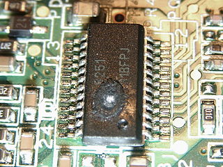
In microelectronics, a dual in-line package is an electronic component package with a rectangular housing and two parallel rows of electrical connecting pins. The package may be through-hole mounted to a printed circuit board (PCB) or inserted in a socket. The dual-inline format was invented by Don Forbes, Rex Rice and Bryant Rogers at Fairchild R&D in 1964, when the restricted number of leads available on circular transistor-style packages became a limitation in the use of integrated circuits. Increasingly complex circuits required more signal and power supply leads ; eventually microprocessors and similar complex devices required more leads than could be put on a DIP package, leading to development of higher-density chip carriers. Furthermore, square and rectangular packages made it easier to route printed-circuit traces beneath the packages.

<span class="mw-page-title-main">Printed circuit board</span> Board to support and connect electronic components

A printed circuit board (PCB), also called printed wiring board (PWB), is a medium used to connect or "wire" components to one another in a circuit. It takes the form of a laminated sandwich structure of conductive and insulating layers: each of the conductive layers is designed with an artwork pattern of traces, planes and other features etched from one or more sheet layers of copper laminated onto and/or between sheet layers of a non-conductive substrate. Electrical components may be fixed to conductive pads on the outer layers in the shape designed to accept the component's terminals, generally by means of soldering, to both electrically connect and mechanically fasten them to it. Another manufacturing process adds vias: plated-through holes that allow interconnections between layers.

<span class="mw-page-title-main">Thermosetting polymer</span> Polymer obtained by irreversibly hardening (curing) a resin

In materials science, a thermosetting polymer, often called a thermoset, is a polymer that is obtained by irreversibly hardening ("curing") a soft solid or viscous liquid prepolymer (resin). Curing is induced by heat or suitable radiation and may be promoted by high pressure or mixing with a catalyst. Heat is not necessarily applied externally, and is often generated by the reaction of the resin with a curing agent. Curing results in chemical reactions that create extensive cross-linking between polymer chains to produce an infusible and insoluble polymer network.

A hermetic seal is any type of sealing that makes a given object airtight. The term originally applied to airtight glass containers, but as technology advanced it applied to a larger category of materials, including rubber and plastics. Hermetic seals are essential to the correct and safe functionality of many electronic and healthcare products. Used technically, it is stated in conjunction with a specific test method and conditions of use.

<span class="mw-page-title-main">Electronic component</span> Discrete device in an electronic system

An electronic component is any basic discrete electronic device or physical entity part of an electronic system used to affect electrons or their associated fields. Electronic components are mostly industrial products, available in a singular form and are not to be confused with electrical elements, which are conceptual abstractions representing idealized electronic components and elements.

<span class="mw-page-title-main">Hybrid integrated circuit</span> Type of miniature electronic circuit

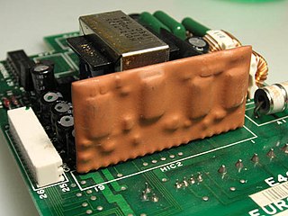
A hybrid integrated circuit (HIC), hybrid microcircuit, hybrid circuit or simply hybrid is a miniaturized electronic circuit constructed of individual devices, such as semiconductor devices and passive components, bonded to a substrate or printed circuit board (PCB). A PCB having components on a Printed Wiring Board (PWB) is not considered a true hybrid circuit according to the definition of MIL-PRF-38534.

Conformal coating is a protective, breathable coating of thin polymeric film applied to printed circuit boards (PCB). It is named as such because it conforms to the contours of the PCB. Conformal coatings are typically applied at 25–250 μm to the electronic circuitry and provide protection against moisture, dust, chemicals, and temperature extremities. More recently, conformal coatings have been used to reduce the formation of whiskers, and can also prevent current bleed between closely positioned components.

<span class="mw-page-title-main">Ceramic capacitor</span> Fixed-value capacitor using ceramic

A ceramic capacitor is a fixed-value capacitor where the ceramic material acts as the dielectric. It is constructed of two or more alternating layers of ceramic and a metal layer acting as the electrodes. The composition of the ceramic material defines the electrical behavior and therefore applications. Ceramic capacitors are divided into two application classes:

Microvias are used as the interconnects between layers in high density interconnect (HDI) substrates and printed circuit boards (PCBs) to accommodate the high input/output (I/O) density of advanced packages. Driven by portability and wireless communications, the electronics industry strives to produce affordable, light, and reliable products with increased functionality. At the electronic component level, this translates to components with increased I/Os with smaller footprint areas, and on the printed circuit board and package substrate level, to the use of high density interconnects (HDIs).

<span class="mw-page-title-main">Integrated passive devices</span>

Integrated passive devices (IPDs), also known as integrated passive components (IPCs) or embedded passive components (EPC), are electronic components where resistors (R), capacitors (C), inductors (L)/coils/chokes, microstriplines, impedance matching elements, baluns or any combinations of them are integrated in the same package or on the same substrate. Sometimes integrated passives can also be called as embedded passives, and still the difference between integrated and embedded passives is technically unclear. In both cases passives are realized in between dielectric layers or on the same substrate.

<span class="mw-page-title-main">Thick-film technology</span>

Thick-film technology is used to produce electronic devices/modules such as surface mount devices modules, hybrid integrated circuits, heating elements, integrated passive devices and sensors. Main manufacturing technique is screen printing (stenciling), which in addition to use in manufacturing electronic devices can also be used for various graphic reproduction targets. It became one of the key manufacturing/miniaturisation techniques of electronic devices/modules during 1950s. Typical film thickness – manufactured with thick film manufacturing processes for electronic devices – is 0.0001 to 0.1 mm.

Reliability of a semiconductor device is the ability of the device to perform its intended function during the intended life of the device in the field.

A semiconductor package is a metal, plastic, glass, or ceramic casing containing one or more discrete semiconductor devices or integrated circuits. Individual components are fabricated on semiconductor wafers before being diced into die, tested, and packaged. The package provides a means for connecting it to the external environment, such as printed circuit board, via leads such as lands, balls, or pins; and protection against threats such as mechanical impact, chemical contamination, and light exposure. Additionally, it helps dissipate heat produced by the device, with or without the aid of a heat spreader. There are thousands of package types in use. Some are defined by international, national, or industry standards, while others are particular to an individual manufacturer.

<span class="mw-page-title-main">Failure of electronic components</span> Ways electronic components fail and prevention measures

Electronic components have a wide range of failure modes. These can be classified in various ways, such as by time or cause. Failures can be caused by excess temperature, excess current or voltage, ionizing radiation, mechanical shock, stress or impact, and many other causes. In semiconductor devices, problems in the device package may cause failures due to contamination, mechanical stress of the device, or open or short circuits.

<span class="mw-page-title-main">Chip carrier</span> Surface mount technology package for integrated circuits

In electronics, a chip carrier is one of several kinds of surface-mount technology packages for integrated circuits. Connections are made on all four edges of a square package; compared to the internal cavity for mounting the integrated circuit, the package overall size is large.

<span class="mw-page-title-main">Co-fired ceramic</span> Integrated circuit package made out of fired ceramic material

Co-fired ceramic devices are monolithic, ceramic microelectronic devices where the entire ceramic support structure and any conductive, resistive, and dielectric materials are fired in a kiln at the same time. Typical devices include capacitors, inductors, resistors, transformers, and hybrid circuits. The technology is also used for robust assembly and packaging of electronic components multi-layer packaging in the electronics industry, such as military electronics, MEMS, microprocessor and RF applications.

Digital image correlation analyses have applications in material property characterization, displacement measurement, and strain mapping. As such, DIC is becoming an increasingly popular tool when evaluating the thermo-mechanical behavior of electronic components and systems.

Glossary of microelectronics manufacturing terms

References

  1. Michael Pecht et al, Electronic Packaging Materials and Their Properties, CRC Press, 2017 ISBN   135183004X ,Preface
  2. Sudo, Toshio & Sasaki, Hideki & Masuda, Norio & Drewniak, James. (2004). Electromagnetic Interference (EMI) of System-on-Package (SOP). Advanced Packaging, IEEE Transactions on. 27. 304 - 314. 10.1109/TADVP.2004.828817.
  3. Nandivada, Venkat (2013-01-16). "Enhance Electronic Performance with Epoxy Compounds". Design World . Retrieved 2023-02-17.
  4. Kelly, Joe (December 2004). "Improving Chip on Board Assembly". empf.com. Archived from the original on 2006-09-23.
  5. Handbook on the Physics and Chemistry of Rare Earths: Including Actinides. Elsevier Science. 1 August 2016. p. 89. ISBN   978-0-444-63705-5.
  6. G. Wu et al. "Study on the shear strength degradation of ACA joints induced by different hygrothermal aging conditions ". Microelectronics Reliability. 2013.