A semiconductor is a material which has an electrical conductivity value falling between that of a conductor, such as copper, and an insulator, such as glass. Its resistivity falls as its temperature rises; metals behave in the opposite way. Its conducting properties may be altered in useful ways by introducing impurities ("doping") into the crystal structure. When two differently doped regions exist in the same crystal, a semiconductor junction is created. The behavior of charge carriers, which include electrons, ions, and electron holes, at these junctions is the basis of diodes, transistors, and most modern electronics. Some examples of semiconductors are silicon, germanium, gallium arsenide, and elements near the so-called "metalloid staircase" on the periodic table. After silicon, gallium arsenide is the second-most common semiconductor and is used in laser diodes, solar cells, microwave-frequency integrated circuits, and others. Silicon is a critical element for fabricating most electronic circuits.

A semiconductor device is an electronic component that relies on the electronic properties of a semiconductor material for its function. Its conductivity lies between conductors and insulators. Semiconductor devices have replaced vacuum tubes in most applications. They conduct electric current in the solid state, rather than as free electrons across a vacuum or as free electrons and ions through an ionized gas.

In electronics, a wafer is a thin slice of semiconductor, such as a crystalline silicon (c-Si), used for the fabrication of integrated circuits and, in photovoltaics, to manufacture solar cells. The wafer serves as the substrate for microelectronic devices built in and upon the wafer. It undergoes many microfabrication processes, such as doping, ion implantation, etching, thin-film deposition of various materials, and photolithographic patterning. Finally, the individual microcircuits are separated by wafer dicing and packaged as an integrated circuit.

Gallium arsenide (GaAs) is a III-V direct band gap semiconductor with a zinc blende crystal structure.

Zone melting is a group of similar methods of purifying crystals, in which a narrow region of a crystal is melted, and this molten zone is moved along the crystal. The molten region melts impure solid at its forward edge and leaves a wake of purer material solidified behind it as it moves through the ingot. The impurities concentrate in the melt, and are moved to one end of the ingot. Zone refining was invented by John Desmond Bernal and further developed by William G. Pfann in Bell Labs as a method to prepare high purity materials, mainly semiconductors, for manufacturing transistors. Its first commercial use was in germanium, refined to one atom of impurity per ten billion, but the process can be extended to virtually any solute–solvent system having an appreciable concentration difference between solid and liquid phases at equilibrium. This process is also known as the float zone process, particularly in semiconductor materials processing.

The Czochralski method, also Czochralski technique or Czochralski process, is a method of crystal growth used to obtain single crystals of semiconductors, metals, salts and synthetic gemstones. The method is named after Polish scientist Jan Czochralski, who invented the method in 1915 while investigating the crystallization rates of metals. He made this discovery by accident: instead of dipping his pen into his inkwell, he dipped it in molten tin, and drew a tin filament, which later proved to be a single crystal.
Epitaxy refers to a type of crystal growth or material deposition in which new crystalline layers are formed with one or more well-defined orientations with respect to the crystalline seed layer. The deposited crystalline film is called an epitaxial film or epitaxial layer. The relative orientation(s) of the epitaxial layer to the seed layer is defined in terms of the orientation of the crystal lattice of each material. For most epitaxial growths, the new layer is usually crystalline and each crystallographic domain of the overlayer must have a well-defined orientation relative to the substrate crystal structure. Epitaxy can involve single-crystal structures, although grain-to-grain epitaxy has been observed in granular films. For most technological applications, single domain epitaxy, which is the growth of an overlayer crystal with one well-defined orientation with respect to the substrate crystal, is preferred. Epitaxy can also play an important role while growing superlattice structures.

Molecular-beam epitaxy (MBE) is an epitaxy method for thin-film deposition of single crystals. MBE is widely used in the manufacture of semiconductor devices, including transistors, and it is considered one of the fundamental tools for the development of nanotechnologies. MBE is used to fabricate diodes and MOSFETs at microwave frequencies, and to manufacture the lasers used to read optical discs.
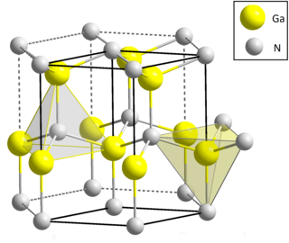
Gallium nitride is a binary III/V direct bandgap semiconductor commonly used in blue light-emitting diodes since the 1990s. The compound is a very hard material that has a Wurtzite crystal structure. Its wide band gap of 3.4 eV affords it special properties for applications in optoelectronic, high-power and high-frequency devices. For example, GaN is the substrate which makes violet (405 nm) laser diodes possible, without requiring nonlinear optical frequency-doubling.
Indium phosphide (InP) is a binary semiconductor composed of indium and phosphorus. It has a face-centered cubic ("zincblende") crystal structure, identical to that of GaAs and most of the III-V semiconductors.
In semiconductor production, doping is the intentional introduction of impurities into an intrinsic semiconductor for the purpose of modulating its electrical, optical and structural properties. The doped material is referred to as an extrinsic semiconductor.
A boule is a single-crystal ingot produced by synthetic means.
An extrinsic semiconductor is one that has been doped; during manufacture of the semiconductor crystal a trace element or chemical called a doping agent has been incorporated chemically into the crystal, for the purpose of giving it different electrical properties than the pure semiconductor crystal, which is called an intrinsic semiconductor. In an extrinsic semiconductor it is these foreign dopant atoms in the crystal lattice that mainly provide the charge carriers which carry electric current through the crystal. The doping agents used are of two types, resulting in two types of extrinsic semiconductor. An electron donor dopant is an atom which, when incorporated in the crystal, releases a mobile conduction electron into the crystal lattice. An extrinsic semiconductor which has been doped with electron donor atoms is called an n-type semiconductor, because the majority of charge carriers in the crystal are negative electrons. An electron acceptor dopant is an atom which accepts an electron from the lattice, creating a vacancy where an electron should be called a hole which can move through the crystal like a positively charged particle. An extrinsic semiconductor which has been doped with electron acceptor atoms is called a p-type semiconductor, because the majority of charge carriers in the crystal are positive holes.
Monocrystalline silicon, more often called single-crystal silicon, in short mono c-Si or mono-Si, is the base material for silicon-based discrete components and integrated circuits used in virtually all modern electronic equipment. Mono-Si also serves as a photovoltaic, light-absorbing material in the manufacture of solar cells.

Crystalline silicon or (c-Si) Is the crystalline forms of silicon, either polycrystalline silicon, or monocrystalline silicon. Crystalline silicon is the dominant semiconducting material used in photovoltaic technology for the production of solar cells. These cells are assembled into solar panels as part of a photovoltaic system to generate solar power from sunlight.
Ultra-high-purity steam, also called the clean steam, UHP steam or high purity water vapor, is used in a variety of industrial manufacturing processes that require oxidation or annealing. These processes include the growth of oxide layers on silicon wafers for the semiconductor industry, originally described by the Deal-Grove model, and for the formation of passivation layers used to improve the light capture ability of crystalline photovoltaic cells. Several methods and technologies can be employed to generate ultra high purity steam, including pyrolysis, bubbling, direct liquid injection and purified steam generation. The level of purity, or the relative lack of contamination, affects the quality of the oxide layer or annealed surface. The method of delivery affects growth rate, uniformity and electrical performance. Oxidation and annealing are common steps in the manufacture of such devices as microelectronics and solar cells.
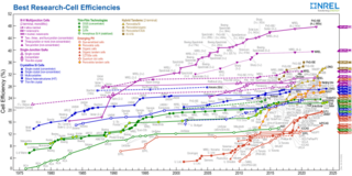
There are currently many research groups active in the field of photovoltaics in universities and research institutions around the world. This research can be categorized into three areas: making current technology solar cells cheaper and/or more efficient to effectively compete with other energy sources; developing new technologies based on new solar cell architectural designs; and developing new materials to serve as more efficient energy converters from light energy into electric current or light absorbers and charge carriers.

Polycrystalline silicon, or multicrystalline silicon, also called polysilicon, poly-Si, or mc-Si, is a high purity, polycrystalline form of silicon, used as a raw material by the solar photovoltaic and electronics industry.

Amorphous silicon (a-Si) is the non-crystalline form of silicon used for solar cells and thin-film transistors in LCDs.
Gas immersion laser doping (GILD) is a method of doping a semiconductor material such as silicon.

