
The metal–oxide–semiconductor field-effect transistor is a type of field-effect transistor (FET), most commonly fabricated by the controlled oxidation of silicon. It has an insulated gate, the voltage of which determines the conductivity of the device. This ability to change conductivity with the amount of applied voltage can be used for amplifying or switching electronic signals. The term metal–insulator–semiconductor field-effect transistor (MISFET) is almost synonymous with MOSFET. Another near-synonym is insulated-gate field-effect transistor (IGFET).
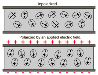
In electromagnetism, a dielectric is an electrical insulator that can be polarised by an applied electric field. When a dielectric material is placed in an electric field, electric charges do not flow through the material as they do in an electrical conductor, because they have no loosely bound, or free, electrons that may drift through the material, but instead they shift, only slightly, from their average equilibrium positions, causing dielectric polarisation. Because of dielectric polarisation, positive charges are displaced in the direction of the field and negative charges shift in the direction opposite to the field. This creates an internal electric field that reduces the overall field within the dielectric itself. If a dielectric is composed of weakly bonded molecules, those molecules not only become polarised, but also reorient so that their symmetry axes align to the field.
In electromagnetism, the absolute permittivity, often simply called permittivity and denoted by the Greek letter ε (epsilon), is a measure of the electric polarizability of a dielectric material. A material with high permittivity polarizes more in response to an applied electric field than a material with low permittivity, thereby storing more energy in the material. In electrostatics, the permittivity plays an important role in determining the capacitance of a capacitor.

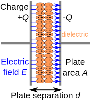
Capacitance is the capability of a material object or device to store electric charge. It is measured by the charge in response to a difference in electric potential, expressed as the ratio of those quantities. Commonly recognized are two closely related notions of capacitance: self capacitance and mutual capacitance. An object that can be electrically charged exhibits self capacitance, for which the electric potential is measured between the object and ground. Mutual capacitance is measured between two components, and is particularly important in the operation of the capacitor, an elementary linear electronic component designed to add capacitance to an electric circuit.
In semiconductor manufacturing, a low-κ is a material with a small relative dielectric constant relative to silicon dioxide. Low-κ dielectric material implementation is one of several strategies used to allow continued scaling of microelectronic devices, colloquially referred to as extending Moore's law. In digital circuits, insulating dielectrics separate the conducting parts from one another. As components have scaled and transistors have gotten closer together, the insulating dielectrics have thinned to the point where charge build up and crosstalk adversely affect the performance of the device. Replacing the silicon dioxide with a low-κ dielectric of the same thickness reduces parasitic capacitance, enabling faster switching speeds and lower heat dissipation. In conversation such materials may be referred to as "low-k" rather than "low-κ" (low-kappa).
Gaussian units constitute a metric system of physical units. This system is the most common of the several electromagnetic unit systems based on cgs (centimetre–gram–second) units. It is also called the Gaussian unit system, Gaussian-cgs units, or often just cgs units. The term "cgs units" is ambiguous and therefore to be avoided if possible: there are several variants of cgs with conflicting definitions of electromagnetic quantities and units.
The threshold voltage, commonly abbreviated as Vth or VGS(th), of a field-effect transistor (FET) is the minimum gate-to-source voltage (VGS) that is needed to create a conducting path between the source and drain terminals. It is an important scaling factor to maintain power efficiency.

In electronics, a common-source amplifier is one of three basic single-stage field-effect transistor (FET) amplifier topologies, typically used as a voltage or transconductance amplifier. The easiest way to tell if a FET is common source, common drain, or common gate is to examine where the signal enters and leaves. The remaining terminal is what is known as "common". In this example, the signal enters the gate, and exits the drain. The only terminal remaining is the source. This is a common-source FET circuit. The analogous bipolar junction transistor circuit may be viewed as a transconductance amplifier or as a voltage amplifier.. As a transconductance amplifier, the input voltage is seen as modulating the current going to the load. As a voltage amplifier, input voltage modulates the current flowing through the FET, changing the voltage across the output resistance according to Ohm's law. However, the FET device's output resistance typically is not high enough for a reasonable transconductance amplifier, nor low enough for a decent voltage amplifier. As seen below in the formula, the voltage gain depends on the load resistance, so it cannot be applied to drive low-resistance devices, such as a speaker. Another major drawback is the amplifier's limited high-frequency response. Therefore, in practice the output often is routed through either a voltage follower, or a current follower, to obtain more favorable output and frequency characteristics. The CS–CG combination is called a cascode amplifier.
In the semiconductor industry, the term high-κ dielectric refers to a material with a high dielectric constant, as compared to silicon dioxide. High-κ dielectrics are used in semiconductor manufacturing processes where they are usually used to replace a silicon dioxide gate dielectric or another dielectric layer of a device. The implementation of high-κ gate dielectrics is one of several strategies developed to allow further miniaturization of microelectronic components, colloquially referred to as extending Moore's Law.
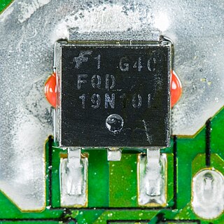
A power MOSFET is a specific type of metal–oxide–semiconductor field-effect transistor (MOSFET) designed to handle significant power levels. Compared to the other power semiconductor devices, such as an insulated-gate bipolar transistor (IGBT) or a thyristor, its main advantages are high switching speed and good efficiency at low voltages. It shares with the IGBT an isolated gate that makes it easy to drive. They can be subject to low gain, sometimes to a degree that the gate voltage needs to be higher than the voltage under control.

In electrical engineering, a capacitor is a device that stores electrical energy by accumulating electric charges on two closely spaced surfaces that are insulated from each other. The capacitor was originally known as the condenser, a term still encountered in a few compound names, such as the condenser microphone. It is a passive electronic component with two terminals.
A gate dielectric is a dielectric used between the gate and substrate of a field-effect transistor. In state-of-the-art processes, the gate dielectric is subject to many constraints, including:
An equivalent oxide thickness usually given in nanometers (nm) is the thickness of silicon oxide film that provides the same electrical performance as that of a high-κ material being used.

A MIS capacitor is a capacitor formed from a layer of metal, a layer of insulating material and a layer of semiconductor material. It gets its name from the initials of the metal-insulator-semiconductor (MIS) structure. As with the MOS field-effect transistor structure, for historical reasons, this layer is also often referred to as a MOS capacitor, but this specifically refers to an oxide insulator material.
A carbon nanotube field-effect transistor (CNTFET) is a field-effect transistor that utilizes a single carbon nanotube (CNT) or an array of carbon nanotubes as the channel material, instead of bulk silicon, as in the traditional MOSFET structure. There have been major developments since CNTFETs were first demonstrated in 1998.

A FET amplifier is an amplifier that uses one or more field-effect transistors (FETs). The most common type of FET amplifier is the MOSFET amplifier, which uses metal–oxide–semiconductor FETs (MOSFETs). The main advantage of a FET used for amplification is that it has very high input impedance and low output impedance.
A quantum field-effect transistor (QFET) or quantum-well field-effect transistor (QWFET) is a type of MOSFET that takes advantage of quantum tunneling to greatly increase the speed of transistor operation by eliminating the traditional transistor's area of electron conduction which typically causes carriers to slow down by a factor of 3000. The result is an increase in logic speed by a factor of 10 with a simultaneous reduction in component power requirement and size also by a factor of 10. It achieves these things through a manufacturing process known as rapid thermal processing (RTP) that uses ultrafine layers of construction materials.
In semiconductor electronics, Dennard scaling, also known as MOSFET scaling, is a scaling law which states roughly that, as transistors get smaller, their power density stays constant, so that the power use stays in proportion with area; both voltage and current scale (downward) with length. The law, originally formulated for MOSFETs, is based on a 1974 paper co-authored by Robert H. Dennard, after whom it is named.
A loop-gap resonator (LGR) is an electromagnetic resonator that operates in the radio and microwave frequency ranges. The simplest LGRs are made from a conducting tube with a narrow slit cut along its length. The LGR dimensions are typically much smaller than the free-space wavelength of the electromagnetic fields at the resonant frequency. Therefore, relatively compact LGRs can be designed to operate at frequencies that are too low to be accessed using, for example, cavity resonators. These structures can have very sharp resonances making them useful for electron spin resonance (ESR) experiments, and precision measurements of electromagnetic material properties.
A ferroelectric field-effect transistor is a type of field-effect transistor that includes a ferroelectric material sandwiched between the gate electrode and source-drain conduction region of the device. Permanent electrical field polarisation in the ferroelectric causes this type of device to retain the transistor's state in the absence of any electrical bias.

