Related Research Articles

A laser is a device that emits light through a process of optical amplification based on the stimulated emission of electromagnetic radiation. The word "laser" is an acronym for "light amplification by stimulated emission of radiation". The first laser was built in 1960 by Theodore H. Maiman at Hughes Research Laboratories, based on theoretical work by Charles Hard Townes and Arthur Leonard Schawlow.

A laser diode is a semiconductor device similar to a light-emitting diode in which a diode pumped directly with electrical current can create lasing conditions at the diode's junction.

Photonics is the physical science and application of light (photon) generation, detection, and manipulation through emission, transmission, modulation, signal processing, switching, amplification, and sensing. Though covering all light's technical applications over the whole spectrum, most photonic applications are in the range of visible and near-infrared light. The term photonics developed as an outgrowth of the first practical semiconductor light emitters invented in the early 1960s and optical fibers developed in the 1970s.

The vertical-cavity surface-emitting laser, or VCSEL, is a type of semiconductor laser diode with laser beam emission perpendicular from the top surface, contrary to conventional edge-emitting semiconductor lasers which emit from surfaces formed by cleaving the individual chip out of a wafer. VCSELs are used in various laser products, including computer mice, fiber optic communications, laser printers, Face ID, and smartglasses.
In semiconductor manufacturing, silicon on insulator (SOI) technology is fabrication of silicon semiconductor devices in a layered silicon–insulator–silicon substrate, to reduce parasitic capacitance within the device, thereby improving performance. SOI-based devices differ from conventional silicon-built devices in that the silicon junction is above an electrical insulator, typically silicon dioxide or sapphire. The choice of insulator depends largely on intended application, with sapphire being used for high-performance radio frequency (RF) and radiation-sensitive applications, and silicon dioxide for diminished short-channel effects in other microelectronics devices. The insulating layer and topmost silicon layer also vary widely with application.
A Raman laser is a specific type of laser in which the fundamental light-amplification mechanism is stimulated Raman scattering. In contrast, most "conventional" lasers rely on stimulated electronic transitions to amplify light.
Quantum cascade lasers (QCLs) are semiconductor lasers that emit in the mid- to far-infrared portion of the electromagnetic spectrum and were first demonstrated by Jerome Faist, Federico Capasso, Deborah Sivco, Carlo Sirtori, Albert Hutchinson, and Alfred Cho at Bell Laboratories in 1994.
An optical waveguide is a physical structure that guides electromagnetic waves in the optical spectrum. Common types of optical waveguides include optical fiber and transparent dielectric waveguides made of plastic and glass.
Nanophotonics or nano-optics is the study of the behavior of light on the nanometer scale, and of the interaction of nanometer-scale objects with light. It is a branch of optics, optical engineering, electrical engineering, and nanotechnology. It often involves dielectric structures such as nanoantennas, or metallic components, which can transport and focus light via surface plasmon polaritons.
A photonic integrated circuit (PIC) or integrated optical circuit is a device that integrates multiple photonic functions and as such is similar to an electronic integrated circuit. The major difference between the two is that a photonic integrated circuit provides functions for information signals imposed on optical wavelengths typically in the visible spectrum or near infrared 850 nm-1650 nm.

Silicon photonics is the study and application of photonic systems which use silicon as an optical medium. The silicon is usually patterned with sub-micrometre precision, into microphotonic components. These operate in the infrared, most commonly at the 1.55 micrometre wavelength used by most fiber optic telecommunication systems. The silicon typically lies on top of a layer of silica in what is known as silicon on insulator (SOI).

Charles H. Henry was an American physicist. He was born in Chicago, Illinois. He received an M.S. degree in physics in 1959 from the University of Chicago, and a Ph.D. degree in physics in 1965 from the University of Illinois, under the direction of Charlie Slichter. In March 2008, he was featured in an article in the Physics Illinois News, a publication of the Physics Department of the University of Illinois.
A quantum well laser is a laser diode in which the active region of the device is so narrow that quantum confinement occurs. Laser diodes are formed in compound semiconductor materials that are able to emit light efficiently. The wavelength of the light emitted by a quantum well laser is determined by the width of the active region rather than just the bandgap of the materials from which it is constructed. This means that much shorter wavelengths can be obtained from quantum well lasers than from conventional laser diodes using a particular semiconductor material. The efficiency of a quantum well laser is also greater than a conventional laser diode due to the stepwise form of its density of states function.

Digital planar holography (DPH) is a method for designing and fabricating miniature components for integrated optics. It was invented by Vladimir Yankov and first published in 2003. The essence of the DPH technology is embedding computer designed digital holograms inside a planar waveguide. Light propagates through the plane of the hologram instead of perpendicularly, allowing for a long interaction path. Benefits of a long interaction path have long been used by volume or thick holograms. Planar configuration of the hologram provider for easier access to the embedded diagram aiding in its manufacture.

Michael Hochberg is an American physicist. He’s authored over 100 peer-reviewed journal articles, has founded several companies, and has been an inventor on over 60 patents. Hochberg's research interests include silicon photonics and large-scale photonic integration. He has worked in a number of application areas, including data communications, biosensing, quantum optics, mid-infrared photonics, optical computing, and machine learning. Much of his work in silicon photonics has been the product of a longstanding series of collaborations with Thomas Baehr-Jones.

The Ferdinand-Braun-Institut, Leibniz-Institut für Höchstfrequenztechnik (FBH) is a research institute, which is a member of the Gottfried Wilhelm Leibniz Scientific Community. The institute is located in Berlin at the Wissenschafts- und Wirtschaftsstandort Adlershof (WISTA), its research activity is applied science in the fields of III-V electronics, photonics, integrated quantum technology and III-V technology
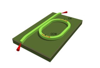
Semiconductor ring lasers (SRLs) are miniature ring laser devices with potential applications in optoelectronics, photonics and all-optical circuits. The first SRLs were developed in the 1980s. Recently, they have been of interest as potential random-access memory storage devices for all-optical computers.

Interband cascade lasers (ICLs) are a type of laser diode that can produce coherent radiation over a large part of the mid-infrared region of the electromagnetic spectrum. They are fabricated from epitaxially-grown semiconductor heterostructures composed of layers of indium arsenide (InAs), gallium antimonide (GaSb), aluminum antimonide (AlSb), and related alloys. These lasers are similar to quantum cascade lasers (QCLs) in several ways. Like QCLs, ICLs employ the concept of bandstructure engineering to achieve an optimized laser design and reuse injected electrons to emit multiple photons. However, in ICLs, photons are generated with interband transitions, rather than the intersubband transitions used in QCLs. Consequently, the rate at which the carriers injected into the upper laser subband thermally relax to the lower subband is determined by interband Auger, radiative, and Shockley-Read carrier recombination. These processes typically occur on a much slower time scale than the longitudinal optical phonon interactions that mediates the intersubband relaxation of injected electrons in mid-IR QCLs. The use of interband transitions allows laser action in ICLs to be achieved at lower electrical input powers than is possible with QCLs.

Semiconductor nanowire lasers are nano-scaled lasers that can be embedded on chips and constitute an advance for computing and information processing applications. Nanowire lasers are coherent light sources as any other laser device, with the advantage of operating at the nanoscale. Built by molecular beam epitaxy, nanowire lasers offer the possibility for direct integration on silicon, and the construction of optical interconnects and data communication at the chip scale. Nanowire lasers are built from III–V semiconductor heterostructures. Their unique 1D configuration and high refractive index allow for low optical loss and recirculation in the active nanowire core region. This enables subwavelength laser sizes of only a few hundred nanometers. Nanowires are Fabry–Perot resonator cavities defined by the end facets of the wire, therefore they do not require polishing or cleaving for high-reflectivity facets as in conventional lasers.
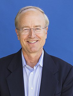
John E. Bowers is an American physicist, engineer, researcher and educator. He is the Fred Kavli Chair in Nanotechnology, the director of the Institute for Energy Efficiency and a distinguished professor in the Departments of Electrical and Computer Engineering and Materials at University of California, Santa Barbara. He is also the deputy director of American Institute of Manufacturing of Integrated Photonics.
References
- ↑ "Hybrid silicon evanescent laser fabricated with a silicon waveguide and III-V offset quantum wells" published in Optics Express, 2005.
- ↑ "A continuous-wave Hybrid AlGaInAs-Silicon Evanescent Laser" published in Photonic Technology Letters, 2006.
- ↑ "Intel® Silicon Photonics: How Does It Work? | Intel".
- ↑ "Home | Bowers".
- ↑ "Hybrid Integrated Platforms for Silicon Photonics," Materials, 3 (3), 1782-1802, March 12, 2010.
- ↑ "Heterogeneously Integrated Photonics", Invited paper, IEEE Nanotechnology Magazine 17, April (2019).
- ↑ “Tutorial: Si/III-V Heterogeneous Integration for Narrow Linewidth Semiconductor Lasers”, APL Photonics 4, 111101 (2019).
- ↑ "Heterogeneous Silicon Photonics Sensing for Autonomous Cars", invited paper, Optics Express 27(3), 3642 (2019).
- ↑ “High Performance Photonic Integrated Circuits on Silicon”, invited paper, JSTQE 25(5) 8300215, Sept. 2019.
- ↑ "An Integrated-Photonics Optical-Frequency Synthesizer," Nature, 557, 81-85, April 25, 2018.
- ↑ “A Distributed Feedback Silicon Evanescent Laser,” Optics Express, 16 (7), 4413-4419, March, 2008.
- ↑ "Mode-locked Silicon Evanescent Lasers," Optics Express, 15 (18), 11225-11233, September, 2007.
- ↑ “Quantum Cascade Laser on Silicon,” Optica, (3)5, 545-551, May 20, 2016.
- ↑ “Interband Cascade Laser on Silicon,” Optica, (5)8, 996-1005, August 16, 2018.
| Basic types | |
|---|---|
| Hybrid types |
|
| Other Types | |
| Theory | |
| Materials |
|