Kenneth L Shepard

Last updated

Kenneth L. Shepard
BornMay, 1966 (1966-05-15)[ citation needed ]
NationalityAmerican
Alma mater Princeton University
Stanford University
Known for electrical engineering, biomedical engineering, nanobiotechnology
Scientific career
Fields Electrical Engineering, Biomedical Engineering, Nanotechnology
Institutions Columbia University

Kenneth L Shepard is an American electrical engineer, nanoscientist, entrepreneur, and the Lau Family Professor of Electrical Engineering and Biomedical Engineering at the Columbia School of Engineering and Applied Science (Columbia). [1] Shepard was born in Bryn Mawr, Pennsylvania.

Contents

He received the B. S. E. degree from Princeton University, Princeton, NJ, in 1987. He was named valedictorian of his graduating class and also received the Phi Beta Kappa prize for the highest academic standing. [2] After graduating from Princeton, he went on to attend Stanford University, Stanford, Ca. where he earned the M. S. and Ph. D. degrees in electrical engineering (with a minor in physics), in 1988 and 1992, respectively. His studies were funded by a fellowship from the Fannie and John Hertz Foundation. [3] His Ph. D. research was also funded by a special "Creativity in Engineering" grant from the National Science Foundation, [4] focused on the physics of nanoscale devices. He was awarded the Hertz Foundation doctoral thesis prize in 1992, given each year to the best Ph. D. thesis from among Hertz Fellows. [5] After receiving his Ph.D., Dr. Shepard joined the IBM Thomas J. Watson Research Center in Yorktown Heights, NY, where he became a Research Staff Member in the VLSI Design Department. At IBM, he was responsible for the design methodology for IBM's first high-performance CMOS microprocessors for the S/390 mainframe, the G4. [6] This design methodology became the basis for subsequent microprocessor designs at IBM. He received IBM Research Division Awards in 1995 and 1997 for his contributions to the S/390 G4 project team.

Entrepreneurial activities

In 1997, Dr. Shepard left IBM, joined Columbia University and simultaneously co-founded CadMOS Design Technology, an EDA start-up. [7] CadMOS pioneered PacifIC and CeltIC, the first tools for large-scale noise analysis of digital integrated circuits. [8] The success of PacifIC and CeltIC led Cadence to acquire CadMOS in 2001. [9]

In 2012, Dr. Shepard co-founded Ferric Semiconductor, a New York City, private venture-backed company that uses patented thin-film inductors to improve power conversion efficiency in integrated circuits. [10] [11] He currently serves as the technical advisor and Chairman of Ferric. In 2014 Ferric was listed as one of the "Silicon 60" hot startups to watch by EE Times [12]

Contributions to science and engineering

Single-molecule electronic methods for biomolecular analysis

Dr. Shepard and his lab have done pioneering work in using electronic detection approaches to probe the properties of single-molecules at high bandwidth. This includes techniques employing nanopores, biological ion channels, and exposed-gate nanoscale transistors for detection. [13] [14] [15] [16]

Other interfaces between CMOS integrated circuits and biological or biomolecular systems

This includes pioneering work on electrochemical imaging [17] and fluorescence imagers, [18] including techniques for imaging redox-active compounds secreted by bacteria and filter-less approaches to fluorescent imaging using CMOS-integrated Geiger-mode single-photon avalanche photodiodes. [19] Other work has focused on interfacing in vitro lipid bilayers and neural tissue with CMOS integrated circuits. [20]

Professor Shepard and his students have done extensive work in the area of integrated power electronics, including techniques for the integration of magnetic core power inductors into a CMOS process. Dr. Shepard founded Ferric, Inc. in 2012 to commercialize the approach, which is now being brought to production manufacturing by TSMC, the world's largest semiconductor foundry. [21] [22] [23] [24]

He and his graduate students did pioneering work in exploiting newly discovered 2D electronic materials, most notably graphene, in electronic devices. This included seminal papers on field-effect transistor operation in graphene, [25] on using boron nitride as a gate dielectric for graphene, [26] and on using graphene-based transistors for flexible electronics [27] [28]

This included the invention of the static noise analysis technique for analyzing signal integrity in integrated circuits and techniques for parasitic extraction. The former work formed the basis for the start-up founded by Dr. Shepard in 1997, CadMOS Design Technology. [29] The latter work formed the basis for techniques currently employed in CAD tools from Cadence and Mentor. [30] He and his students also did pioneering work on the development of resonant clocking including the patent on the technique, which is widely used in industry. [31] [32]

Related Research Articles

<span class="mw-page-title-main">Integrated circuit</span> Electronic circuit formed on a small, flat piece of semiconductor material

An integrated circuit (IC), also known as a microchip, computer chip, or simply chip, is a small electronic device made up of multiple interconnected electronic components such as transistors, resistors, and capacitors. These components are etched onto a small piece of semiconductor material, usually silicon. Integrated circuits are used in a wide range of electronic devices, including computers, smartphones, and televisions, to perform various functions such as processing and storing information. They have greatly impacted the field of electronics by enabling device miniaturization and enhanced functionality.

<span class="mw-page-title-main">Very-large-scale integration</span> Creating an integrated circuit by combining many transistors into a single chip

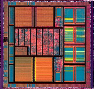
Very-large-scale integration (VLSI) is the process of creating an integrated circuit (IC) by combining millions or billions of MOS transistors onto a single chip. VLSI began in the 1970s when MOS integrated circuit chips were developed and then widely adopted, enabling complex semiconductor and telecommunication technologies. The microprocessor and memory chips are VLSI devices.

<span class="mw-page-title-main">CMOS</span> Technology for constructing integrated circuits

Complementary metal–oxide–semiconductor is a type of metal–oxide–semiconductor field-effect transistor (MOSFET) fabrication process that uses complementary and symmetrical pairs of p-type and n-type MOSFETs for logic functions. CMOS technology is used for constructing integrated circuit (IC) chips, including microprocessors, microcontrollers, memory chips, and other digital logic circuits. CMOS technology is also used for analog circuits such as image sensors, data converters, RF circuits, and highly integrated transceivers for many types of communication.

SiGe, or silicon–germanium, is an alloy with any molar ratio of silicon and germanium, i.e. with a molecular formula of the form Si1−xGex. It is commonly used as a semiconductor material in integrated circuits (ICs) for heterojunction bipolar transistors or as a strain-inducing layer for CMOS transistors. IBM introduced the technology into mainstream manufacturing in 1989. This relatively new technology offers opportunities in mixed-signal circuit and analog circuit IC design and manufacture. SiGe is also used as a thermoelectric material for high-temperature applications (>700 K).

In computer engineering, a logic family is one of two related concepts:

<span class="mw-page-title-main">Mixed-signal integrated circuit</span> Integrated circuit

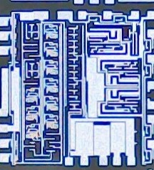
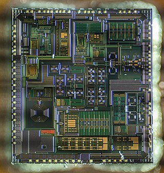
A mixed-signal integrated circuit is any integrated circuit that has both analog circuits and digital circuits on a single semiconductor die. Their usage has grown dramatically with the increased use of cell phones, telecommunications, portable electronics, and automobiles with electronics and digital sensors.

<span class="mw-page-title-main">Depletion-load NMOS logic</span> Form of digital logic family in integrated circuits

In integrated circuits, depletion-load NMOS is a form of digital logic family that uses only a single power supply voltage, unlike earlier NMOS logic families that needed more than one different power supply voltage. Although manufacturing these integrated circuits required additional processing steps, improved switching speed and the elimination of the extra power supply made this logic family the preferred choice for many microprocessors and other logic elements.

<span class="mw-page-title-main">Active-pixel sensor</span> Image sensor, consisting of an integrated circuit

An active-pixel sensor (APS) is an image sensor, which was invented by Peter J.W. Noble in 1968, where each pixel sensor unit cell has a photodetector and one or more active transistors. In a metal–oxide–semiconductor (MOS) active-pixel sensor, MOS field-effect transistors (MOSFETs) are used as amplifiers. There are different types of APS, including the early NMOS APS and the now much more common complementary MOS (CMOS) APS, also known as the CMOS sensor. CMOS sensors are used in digital camera technologies such as cell phone cameras, web cameras, most modern digital pocket cameras, most digital single-lens reflex cameras (DSLRs), mirrorless interchangeable-lens cameras (MILCs), and lensless imaging for cells.

<span class="mw-page-title-main">Technology CAD</span>

Technology computer-aided design is a branch of electronic design automation (EDA) that models semiconductor fabrication and semiconductor device operation. The modeling of the fabrication is termed process TCAD, while the modeling of the device operation is termed device TCAD. Included are the modelling of process steps, and modelling of the behavior of the electrical devices based on fundamental physics, such as the doping profiles of the devices. TCAD may also include the creation of "compact models", which try to capture the electrical behavior of such devices but do not generally derive them from the underlying physics. SPICE simulator itself is usually considered as part of EDA rather than TCAD.

<span class="mw-page-title-main">Semiconductor device modeling</span> Modeling semiconductor behavior

Semiconductor device modeling creates models for the behavior of the electrical devices based on fundamental physics, such as the doping profiles of the devices. It may also include the creation of compact models, which try to capture the electrical behavior of such devices but do not generally derive them from the underlying physics. Normally it starts from the output of a semiconductor process simulation.

<span class="mw-page-title-main">Electric (software)</span> Electronic design automation software tool

The Electric VLSI Design System is an EDA tool written in the early 1980s by Steven M. Rubin. Electric is used to construct logic wire schematics and to perform analysis of integrated circuit layout. It can also handle hardware description languages such as VHDL and Verilog. The system has many analysis and synthesis tools, including design rule checking, simulation, routing, Layout vs. Schematic, logical effort, and more.

<span class="mw-page-title-main">Asad Abidi</span> Pakistani-American electrical engineer

Asad Ali Abidi is a Pakistani-American electrical engineer. He serves as a tenured professor at University of California, Los Angeles, and is the inaugural holder of the Abdus Salam Chair at the Lahore University of Management Sciences (LUMS). He is best known for pioneering RF CMOS technology during the late 1980s to early 1990s. As of 2008, the radio transceivers in all wireless networking devices and modern mobile phones are mass-produced as RF CMOS devices.

<span class="mw-page-title-main">Random-access memory</span> Form of computer data storage

Random-access memory is a form of electronic computer memory that can be read and changed in any order, typically used to store working data and machine code. A random-access memory device allows data items to be read or written in almost the same amount of time irrespective of the physical location of data inside the memory, in contrast with other direct-access data storage media, where the time required to read and write data items varies significantly depending on their physical locations on the recording medium, due to mechanical limitations such as media rotation speeds and arm movement.

In electronics, pass transistor logic (PTL) describes several logic families used in the design of integrated circuits. It reduces the count of transistors used to make different logic gates, by eliminating redundant transistors. Transistors are used as switches to pass logic levels between nodes of a circuit, instead of as switches connected directly to supply voltages. This reduces the number of active devices, but has the disadvantage that the difference of the voltage between high and low logic levels decreases at each stage. Each transistor in series is less saturated at its output than at its input. If several devices are chained in series in a logic path, a conventionally constructed gate may be required to restore the signal voltage to the full value. By contrast, conventional CMOS logic switches transistors so the output connects to one of the power supply rails, so logic voltage levels in a sequential chain do not decrease. Simulation of circuits may be required to ensure adequate performance.

<span class="mw-page-title-main">Ian A. Young</span> American electrical engineer

Ian A. Young is an Intel engineer. Young is a co-author of 50 research papers, and has 71 patents in switched capacitor circuits, DRAM, SRAM, BiCMOS, x86 clocking, Photonics and spintronics.

<span class="mw-page-title-main">Field-effect transistor</span> Type of transistor

The field-effect transistor (FET) is a type of transistor that uses an electric field to control the flow of current in a semiconductor. It comes in two types: junction FET (JFET) and metal-oxide-semiconductor FET (MOSFET). FETs have three terminals: source, gate, and drain. FETs control the flow of current by the application of a voltage to the gate, which in turn alters the conductivity between the drain and source.

RF CMOS is a metal–oxide–semiconductor (MOS) integrated circuit (IC) technology that integrates radio-frequency (RF), analog and digital electronics on a mixed-signal CMOS RF circuit chip. It is widely used in modern wireless telecommunications, such as cellular networks, Bluetooth, Wi-Fi, GPS receivers, broadcasting, vehicular communication systems, and the radio transceivers in all modern mobile phones and wireless networking devices. RF CMOS technology was pioneered by Pakistani engineer Asad Ali Abidi at UCLA during the late 1980s to early 1990s, and helped bring about the wireless revolution with the introduction of digital signal processing in wireless communications. The development and design of RF CMOS devices was enabled by van der Ziel's FET RF noise model, which was published in the early 1960s and remained largely forgotten until the 1990s.

Lawrence Pileggi is the Coraluppi Head and Tanoto Professor of Electrical and Computer Engineering at Carnegie Mellon University. He is a specialist in the automation of integrated circuits, and developing software tools for the optimization of power grids. Pileggi's research has been cited thousands of times in engineering papers.

References

  1. "Kenneth L. Shepard Named Lau Family Professsor of Electrical Engineering | the Fu Foundation School of Engineering & Applied Science - Columbia University". Archived from the original on June 21, 2016. Retrieved July 4, 2016.
  2. "Princeton Weekly Bulletin 22 June 1987 — Princeton Periodicals".
  3. "Kenneth L. Shepard". hertzfoundation.org. Archived from the original on September 17, 2015.
  4. "Princeton Weekly Bulletin 22 June 1987 — Princeton Periodicals".
  5. "Thesis Prize Winners". hertzfoundation.org. Archived from the original on November 5, 2012.
  6. Shepard, K.L.; Carey, S.; Beece, D.K.; Hatch, R.; Northrop, G. (1997). "Design methodology for the high-performance G4 S/390 microprocessor". Proceedings International Conference on Computer Design VLSI in Computers and Processors. pp. 232–240. doi:10.1109/ICCD.1997.628873. ISBN   0-8186-8206-X. S2CID   13009336.
  7. "CadMOS Secures $5 Million in Second Round Funding; Andrew Yang Added to the Company's Board of Directors. - Free Online Library". Archived from the original on August 20, 2016. Retrieved July 4, 2016.
  8. "Texas Instruments Successfully Performs Noise Immunity Validation of a DSP Design With CadMOS' PacifIC. - Free Online Library". www.thefreelibrary.com. Archived from the original on August 20, 2016.
  9. "Cadence Acquires Cadmos". EE Times. January 5, 2001. Retrieved March 3, 2024.
  10. "Company".
  11. Sturcken, Noah; Davies, Ryan; Wu, Hao; Lekas, Michael; Shepard, Kenneth; Cheng, K. W.; Chen, C. C.; Su, Y. S.; Tsai, C. Y.; Wu, K. D.; Wu, J. Y.; Wang, Y. C.; Liu, K. C.; Hsu, C. C.; Chang, C. L.; Hua, W. C.; Kalnitsky, Alex (2015). "Magnetic thin-film inductors for monolithic integration with CMOS". 2015 IEEE International Electron Devices Meeting (IEDM). pp. 11.4.1–11.4.4. doi:10.1109/IEDM.2015.7409676. ISBN   978-1-4673-9894-7. S2CID   18463194.
  12. "EE Times Silicon 60: Hot Startups to Watch". July 15, 2014.
  13. Sorgenfrei S, Chiu CY, Gonzalez RL Jr, Yu YJ, Kim P, Nuckolls C, Shepard KL. Label-free single-molecule detection of DNA-hybridization kinetics with a carbon nanotube field-effect transistor. Nat Nanotechnol. 2011 Feb;6(2):126-32. PMID   21258331; PMC   3783941.
  14. Sorgenfrei S, Chiu CY, Johnston M, Nuckolls C, Shepard KL. Debye screening in single-molecule carbon nanotube field-effect sensors. Nano Lett. 2011 Sep 14;11(9):3739-43. PMID   21806018; PMC   3735439.
  15. Rosenstein JK, Wanunu M, Merchant CA, Drndic M, Shepard KL. Integrated nanopore sensing platform with sub-microsecond temporal resolution. Nat Methods. 2012 Mar 18;9(5):487-92. PMID   22426489; PMC   3648419.
  16. Rosenstein JK, Ramakrishnan S, Roseman J, Shepard KL. Single ion channel recordings with CMOS-anchored lipid membranes. Nano Lett. 2013 Jun 12;13(6):2682-6. PMID   23634707; PMC   3683112.
  17. Levine PM, Gong P, Levicky R, Shepard KL. Active CMOS Sensor Array for Electrochemical Biomolecular Detection. IEEE Journal of Solid-State Circuits. 2008 August; 43(8).
  18. Huang TC, Sorgenfrei S, Gong P, Levicky R, Shepard KL. A 0.18-μm CMOS Array Sensor for Integrated Time-Resolved Fluorescence Detection. IEEE Journal of Solid-State Circuits. 2009 May;44(5):1644-1654. PMID   20436922; PMC   2860634.
  19. Field RM, Realov S, Shepard KL. A 100-fps, Time-Correlated Single-PhotonCounting- Based Fluorescence-Lifetime Imager in 130-nm CMOS. IEEE Journal of Solid-State Circuits. 2014 January 02; 49(4).
  20. Bellin DL, Sakhtah H, Rosenstein JK, Levine PM, Thimot J, Emmett K, Dietrich LE, Shepard KL. Integrated circuit-based electrochemical sensor for spatially resolved detection of redox-active metabolites in biofilms. Nat Commun. 2014;5:3256. PMID   24510163; PMC   3969851.
  21. Sturcken N, Petracca M, Warren S, Mantovani P, Carloni LP, Peterchev AV, Shepard KL. A Switched- Inductor Integrated Voltage Regulator With Nonlinear Feedback and Network-on- Chip Load in 45 nm SOI. IEEE Journal of Solid-State Circuits. 2012 August; 47(8).
  22. Sturcken N, O'Sullivan E, Wang N, Herget P, Webb B, Romankiw L, Petracca M, Davies R, Fontana R, Decad G, Kymissis I, Peterchev A, Carloni L, Gallagher W, Shepard KL. A 2.5D Integrated Voltage Regulator Using Coupled-Magnetic- Core Inductors on Silicon Interposer. IEEE Journal of Solid-State Circuits. 2013 January; 48(1).
  23. Davies RP, Cheng C, Sturcken N, Bailey WE, Shepard KL. Coupled Inductors With Crossed Anisotropy CoZrTz/SiO2Multilayer Cores. IEEE Transactions on Magnetics. 2013 July; 49(7).
  24. Tien K, Sturcken N, Wang N, Nah J, Dang B, O'Sullivan E, Andry P, Petracca M, Carloni L, Gallagher W, Shepard KL. An 82%-Efficient Multiphase Voltage-Regulator 3D Interposer with On-Chip Magnetic Inductors. VLSI Technology (VLSI Technology), 2015 Symposium on; 2015 June; Kyoto, Japan.
  25. Meric I, Han MY, Young AF, Ozyilmaz B, Kim P, Shepard KL. Current saturation in zero-bandgap, top-gated graphene field-effect transistors. Nat Nanotechnol. 2008 Nov;3(11):654-9. PMID   18989330.
  26. Dean CR, Young AF, Meric I, Lee C, Wang L, Sorgenfrei S, Watanabe K, Taniguchi T, Kim P, Shepard KL, Hone J. Boron nitride substrates for high-quality graphene electronics. Nat Nanotechnol. 2010 Oct;5(10):722-6. PMID   20729834.
  27. Petrone N, Meric I, Hone J, Shepard KL. Graphene field-effect transistors with gigahertz-frequency power gain on flexible substrates. Nano Lett. 2013 Jan 9;13(1):121-5. PMID   23256606.
  28. Wang L, Meric I, Huang PY, Gao Q, Gao Y, Tran H, Taniguchi T, Watanabe K, Campos LM, Muller DA, Guo J, Kim P, Hone J, Shepard KL, Dean CR. One-dimensional electrical contact to a two-dimensional material. Science. 2013 Nov 1;342(6158):614-7. PMID   24179223.
  29. Shepard, K.L.; Narayanan, V.; Rose, R. (1999). "Harmony: Static noise analysis of deep submicron digital integrated circuits". IEEE Transactions on Computer-Aided Design of Integrated Circuits and Systems. 18 (8): 1132–1150. doi:10.1109/43.775633.
  30. Shepard, K.L.; Zhong Tian (2000). "Return-limited inductances: A practical approach to on-chip inductance extraction". IEEE Transactions on Computer-Aided Design of Integrated Circuits and Systems. 19 (4): 425–436. doi:10.1109/43.838992.
  31. Chan, S. C.; Shepard, K. L.; Restle, P. J. (2005). "Uniform-phase uniform-amplitude resonant-load global clock distributions". IEEE Journal of Solid-State Circuits. 40 (1): 102. Bibcode:2005IJSSC..40..102C. doi:10.1109/JSSC.2004.838005. S2CID   16239014.
  32. "Resonant clock distribution for very large scale integrated circuits".