
Semiconductor device fabrication is the process used to manufacture semiconductor devices, typically integrated circuits (ICs) such as computer processors, microcontrollers, and memory chips that are present in everyday electronic devices. It is a multiple-step photolithographic and physio-chemical process during which electronic circuits are gradually created on a wafer, typically made of pure single-crystal semiconducting material. Silicon is almost always used, but various compound semiconductors are used for specialized applications.

A semiconductor device is an electronic component that relies on the electronic properties of a semiconductor material for its function. Its conductivity lies between conductors and insulators. Semiconductor devices have replaced vacuum tubes in most applications. They conduct electric current in the solid state, rather than as free electrons across a vacuum or as free electrons and ions through an ionized gas.

The metal–oxide–semiconductor field-effect transistor is a type of field-effect transistor (FET), most commonly fabricated by the controlled oxidation of silicon. It has an insulated gate, the voltage of which determines the conductivity of the device. This ability to change conductivity with the amount of applied voltage can be used for amplifying or switching electronic signals. The term metal–insulator–semiconductor field-effect transistor (MISFET) is almost synonymous with MOSFET. Another near-synonym is insulated-gate field-effect transistor (IGFET).
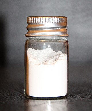
Silicon dioxide, also known as silica, is an oxide of silicon with the chemical formula SiO2, commonly found in nature as quartz. In many parts of the world, silica is the major constituent of sand. Silica is abundant as it comprises several minerals and as a synthetic products. All forms are white or colorless, although impure samples can be colored.

Gallium arsenide (GaAs) is a III-V direct band gap semiconductor with a zinc blende crystal structure.
In semiconductor technology, copper interconnects are interconnects made of copper. They are used in silicon integrated circuits (ICs) to reduce propagation delays and power consumption. Since copper is a better conductor than aluminium, ICs using copper for their interconnects can have interconnects with narrower dimensions, and use less energy to pass electricity through them. Together, these effects lead to ICs with better performance. They were first introduced by IBM, with assistance from Motorola, in 1997.
In semiconductor manufacturing, silicon on insulator (SOI) technology is fabrication of silicon semiconductor devices in a layered silicon–insulator–silicon substrate, to reduce parasitic capacitance within the device, thereby improving performance. SOI-based devices differ from conventional silicon-built devices in that the silicon junction is above an electrical insulator, typically silicon dioxide or sapphire. The choice of insulator depends largely on intended application, with sapphire being used for high-performance radio frequency (RF) and radiation-sensitive applications, and silicon dioxide for diminished short-channel effects in other microelectronics devices. The insulating layer and topmost silicon layer also vary widely with application.
In semiconductor manufacturing, a low-κ is a material with a small relative dielectric constant relative to silicon dioxide. Low-κ dielectric material implementation is one of several strategies used to allow continued scaling of microelectronic devices, colloquially referred to as extending Moore's law. In digital circuits, insulating dielectrics separate the conducting parts from one another. As components have scaled and transistors have gotten closer together, the insulating dielectrics have thinned to the point where charge build up and crosstalk adversely affect the performance of the device. Replacing the silicon dioxide with a low-κ dielectric of the same thickness reduces parasitic capacitance, enabling faster switching speeds and lower heat dissipation. In conversation such materials may be referred to as "low-k" rather than "low-κ" (low-kappa).

The planar process is a manufacturing process used in the semiconductor industry to build individual components of a transistor, and in turn, connect those transistors together. It is the primary process by which silicon integrated circuit chips are built, and it is the most commonly used method of producing junctions during the manufacture of semiconductor devices. The process utilizes the surface passivation and thermal oxidation methods.
Chemical mechanical polishing (CMP) is a process of smoothing surfaces with the combination of chemical and mechanical forces. It can be thought of as a hybrid of chemical etching and free abrasive polishing. It is used in the semiconductor industry to polish semiconductor wafers as part of the integrated circuit manufacturing process.
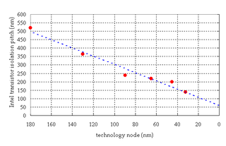
Shallow trench isolation (STI), also known as box isolation technique, is an integrated circuit feature which prevents electric current leakage between adjacent semiconductor device components. STI is generally used on CMOS process technology nodes of 250 nanometers and smaller. Older CMOS technologies and non-MOS technologies commonly use isolation based on LOCOS.
Charge trap flash (CTF) is a semiconductor memory technology used in creating non-volatile NOR and NAND flash memory. It is a type of floating-gate MOSFET memory technology, but differs from the conventional floating-gate technology in that it uses a silicon nitride film to store electrons rather than the doped polycrystalline silicon typical of a floating-gate structure. This approach allows memory manufacturers to reduce manufacturing costs five ways:
- Fewer process steps are required to form a charge storage node
- Smaller process geometries can be used
- Multiple bits can be stored on a single flash memory cell
- Improved reliability
- Higher yield since the charge trap is less susceptible to point defects in the tunnel oxide layer
In semiconductor electronics fabrication technology, a self-aligned gate is a transistor manufacturing approach whereby the gate electrode of a MOSFET is used as a mask for the doping of the source and drain regions. This technique ensures that the gate is naturally and precisely aligned to the edges of the source and drain.

In microfabrication, thermal oxidation is a way to produce a thin layer of oxide on the surface of a wafer. The technique forces an oxidizing agent to diffuse into the wafer at high temperature and react with it. The rate of oxide growth is often predicted by the Deal–Grove model. Thermal oxidation may be applied to different materials, but most commonly involves the oxidation of silicon substrates to produce silicon dioxide.
Ultra-high-purity steam, also called the clean steam, UHP steam or high purity water vapor, is used in a variety of industrial manufacturing processes that require oxidation or annealing. These processes include the growth of oxide layers on silicon wafers for the semiconductor industry, originally described by the Deal-Grove model, and for the formation of passivation layers used to improve the light capture ability of crystalline photovoltaic cells. Several methods and technologies can be employed to generate ultra high purity steam, including pyrolysis, bubbling, direct liquid injection, and purified steam generation. The level of purity, or the relative lack of contamination, affects the quality of the oxide layer or annealed surface. The method of delivery affects growth rate, uniformity, and electrical performance. Oxidation and annealing are common steps in the manufacture of such devices as microelectronics and solar cells.
Direct bonding, or fusion bonding, describes a wafer bonding process without any additional intermediate layers. The bonding process is based on chemical bonds between two surfaces of any material possible meeting numerous requirements. These requirements are specified for the wafer surface as sufficiently clean, flat and smooth. Otherwise unbonded areas so called voids, i.e. interface bubbles, can occur.
Eutectic bonding, also referred to as eutectic soldering, describes a wafer bonding technique with an intermediate metal layer that can produce a eutectic system. Those eutectic metals are alloys that transform directly from solid to liquid state, or vice versa from liquid to solid state, at a specific composition and temperature without passing a two-phase equilibrium, i.e. liquid and solid state. The fact that the eutectic temperature can be much lower than the melting temperature of the two or more pure elements can be important in eutectic bonding.
Mohamed M. Atalla was an Egyptian-American engineer, physicist, cryptographer, inventor and entrepreneur. He was a semiconductor pioneer who made important contributions to modern electronics. He is best known for the inventing the MOSFET in 1959, which along with Atalla's earlier surface passivation processes, had a significant impact on the development of the electronics industry. He is also known as the founder of the data security company Atalla Corporation, founded in 1972. He received the Stuart Ballantine Medal and was inducted into the National Inventors Hall of Fame for his important contributions to semiconductor technology as well as data security.

The field-effect transistor (FET) is a type of transistor that uses an electric field to control the flow of current in a semiconductor. It comes in two types: junction FET (JFET) and metal-oxide-semiconductor FET (MOSFET). FETs have three terminals: source, gate, and drain. FETs control the flow of current by the application of a voltage to the gate, which in turn alters the conductivity between the drain and source.
Low-temperature polycrystalline silicon (LTPS) is polycrystalline silicon that has been synthesized at relatively low temperatures compared to in traditional methods. LTPS is important for display industries, since the use of large glass panels prohibits exposure to deformative high temperatures. More specifically, the use of polycrystalline silicon in thin-film transistors (LTPS-TFT) has high potential for large-scale production of electronic devices like flat panel LCD displays or image sensors.
